Refine search
Actions for selected content:
106116 results in Materials Science

Fabrication of amorphous Co–Cr–B and catalytic sodium borohydride hydrolysis for hydrogen generation
-
- Journal:
- Journal of Materials Research / Volume 35 / Issue 3 / 14 February 2020
- Published online by Cambridge University Press:
- 17 January 2020, pp. 281-288
- Print publication:
- 14 February 2020
-
- Article
- Export citation
Effect of LPHT annealing on interface characteristics between HPHT Ib diamond substrates and homoepitaxial CVD diamond layers
-
- Journal:
- Journal of Materials Research / Volume 35 / Issue 5 / 16 March 2020
- Published online by Cambridge University Press:
- 17 January 2020, pp. 527-536
- Print publication:
- 16 March 2020
-
- Article
- Export citation
-
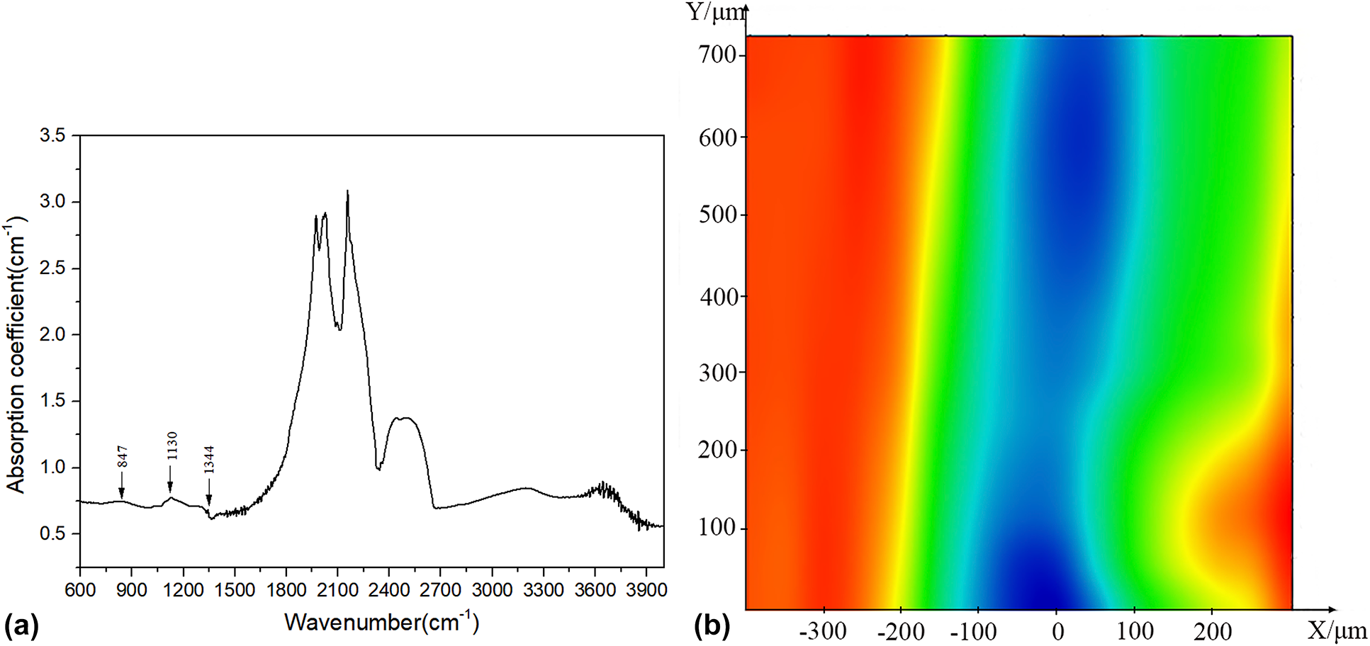
To study the interface characteristics between substrates and homoepitaxially grown single crystalline diamond layers, the high-pressure/high-temperature Ib diamond seeds with homoepitaxial diamond layers were annealed by low-pressure/high-temperature treatment in a hydrogen environment. The stress evolution and related impurity transformation near the interface were characterized by Raman spectroscopy, photoluminescence, and micro-infrared spectroscopy before and after annealing. It is found that the stress is the smallest in a 100 μm wide zone near the interface, accompanying with the similar change in substitutional nitrogen (Ns) concentration. After annealing at 1050 °C, 1250 °C, and 1450 °C, the local compressive stress is released gradually with temperature change. It is decreased by 1.03 GPa in maximum after annealing at 1450 °C. The concentration of nitrogen–vacancy (NV) complexes in the chemical vapor deposition (CVD) layer is dramatically reduced at 1450 °C. The value of ${{I_{{\rm{NV}}^ \hbox- } } \mathord{\left/ {\vphantom {{I_{{\rm{NV}}^ - } } {I_{{\rm{diamond}}} }}} \right. \kern-\nulldelimiterspace} {I_{{\rm{diamond}}} }}$ decreases much more than ${{I_{{\rm{NV}}^0 } } \mathord{\left/ {\vphantom {{I_{{\rm{NV}}^0 } } {I_{{\rm{diamond}}} }}} \right. \kern-\nulldelimiterspace} {I_{{\rm{diamond}}} }}$ in the CVD layer, which is due to the lower stability of NV− compared with NV0 at high temperature.


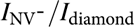
Controllable atomic layer deposition coatings to boost the performance of LiMnxCoyNi1−x−yO2 in lithium-ion batteries: A review
-
- Journal:
- Journal of Materials Research / Volume 35 / Issue 7 / 14 April 2020
- Published online by Cambridge University Press:
- 17 January 2020, pp. 762-774
- Print publication:
- 14 April 2020
-
- Article
-
- You have access
- HTML
- Export citation

Effect of ceramic particle size on densification behavior, microstructure formation, and performance of TiB2-reinforced Al-based composites prepared by selective laser melting
-
- Journal:
- Journal of Materials Research / Volume 35 / Issue 6 / 30 March 2020
- Published online by Cambridge University Press:
- 17 January 2020, pp. 559-570
- Print publication:
- 30 March 2020
-
- Article
- Export citation
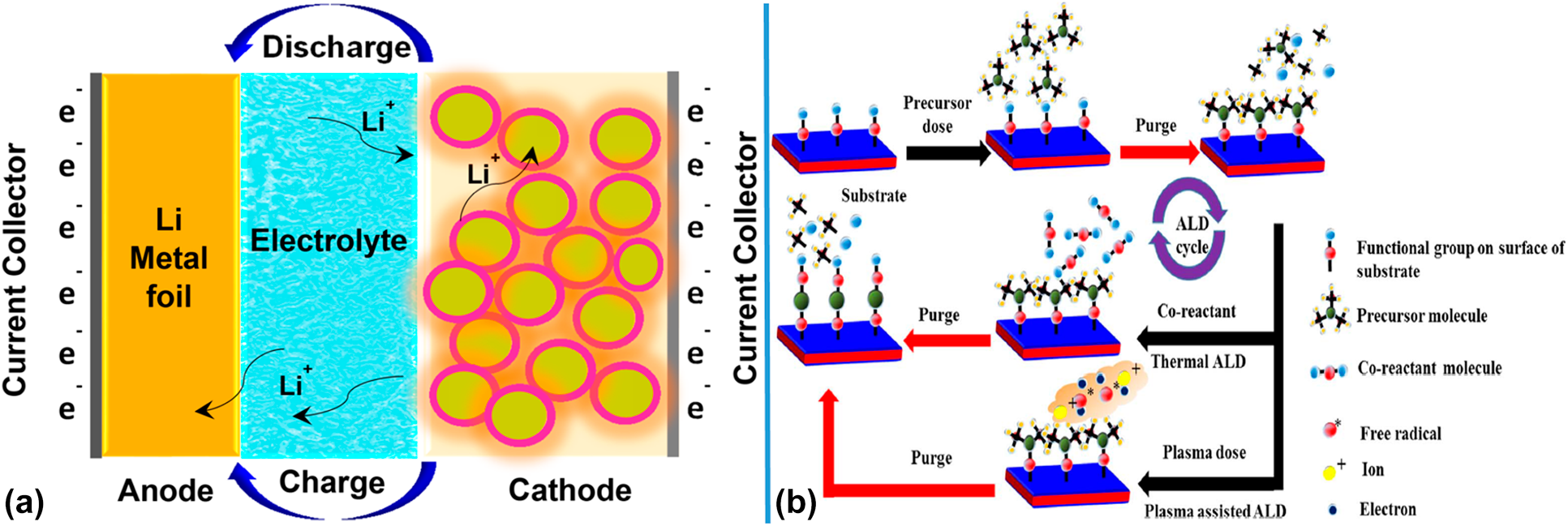
Enhancement of the optical properties of copper sulfate crystal by the influence of shock waves
-
- Journal:
- Journal of Materials Research / Volume 35 / Issue 4 / 28 February 2020
- Published online by Cambridge University Press:
- 17 January 2020, pp. 391-400
- Print publication:
- 28 February 2020
-
- Article
- Export citation

Atomistic kinetic Monte Carlo—Embedded atom method simulation on growth and morphology of Cu–Zn–Sn precursor of Cu2ZnSnS4 solar cells
-
- Journal:
- Journal of Materials Research / Volume 35 / Issue 3 / 14 February 2020
- Published online by Cambridge University Press:
- 17 January 2020, pp. 252-262
- Print publication:
- 14 February 2020
-
- Article
- Export citation
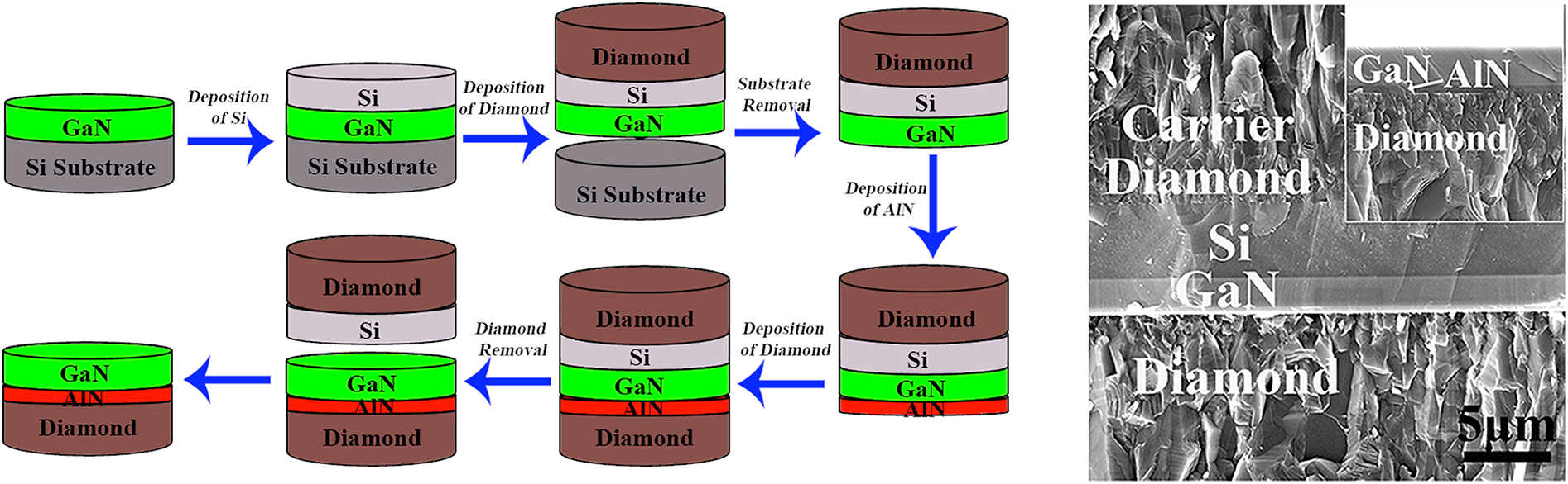
Enhancement of diamond seeding on aluminum nitride dielectric by electrostatic adsorption for GaN-on-diamond preparation
-
- Journal:
- Journal of Materials Research / Volume 35 / Issue 5 / 16 March 2020
- Published online by Cambridge University Press:
- 17 January 2020, pp. 508-515
- Print publication:
- 16 March 2020
-
- Article
- Export citation
Crystal structures of two polymorphs of alclometasone dipropionate, C28H37ClO7
-
- Journal:
- Powder Diffraction / Volume 35 / Issue 1 / March 2020
- Published online by Cambridge University Press:
- 15 January 2020, pp. 45-52
-
- Article
- Export citation
JMR volume 35 issue 1 Cover and Back matter
-
- Journal:
- Journal of Materials Research / Volume 35 / Issue 1 / 14 January 2020
- Published online by Cambridge University Press:
- 14 January 2020, pp. b1-b3
- Print publication:
- 14 January 2020
-
- Article
-
- You have access
- Export citation

Effects of nanoporous Au on ATP synthase
-
- Journal:
- MRS Communications / Volume 10 / Issue 1 / March 2020
- Published online by Cambridge University Press:
- 14 January 2020, pp. 173-178
- Print publication:
- March 2020
-
- Article
- Export citation
Announcement
-
- Journal:
- Journal of Materials Research / Volume 35 / Issue 1 / 14 January 2020
- Published online by Cambridge University Press:
- 14 January 2020, p. 1
- Print publication:
- 14 January 2020
-
- Article
-
- You have access
- HTML
- Export citation

Growing field of materials informatics: databases and artificial intelligence
-
- Journal:
- MRS Communications / Volume 10 / Issue 1 / March 2020
- Published online by Cambridge University Press:
- 14 January 2020, pp. 1-10
- Print publication:
- March 2020
-
- Article
- Export citation

Effects of an interfacial layer on stress relaxation mechanisms active in the Cu–Si thin film system during thermal cycling
-
- Journal:
- MRS Communications / Volume 10 / Issue 1 / March 2020
- Published online by Cambridge University Press:
- 14 January 2020, pp. 164-172
- Print publication:
- March 2020
-
- Article
- Export citation
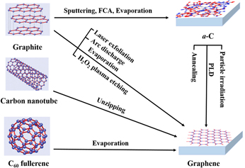
A review of graphene synthesis by indirect and direct deposition methods
-
- Journal:
- Journal of Materials Research / Volume 35 / Issue 1 / 14 January 2020
- Published online by Cambridge University Press:
- 14 January 2020, pp. 76-89
- Print publication:
- 14 January 2020
-
- Article
- Export citation

Design space visualization for guiding investments in biodegradable and sustainably sourced materials
-
- Journal:
- MRS Communications / Volume 10 / Issue 1 / March 2020
- Published online by Cambridge University Press:
- 14 January 2020, pp. 18-24
- Print publication:
- March 2020
-
- Article
-
- You have access
- Open access
- HTML
- Export citation
JMR volume 35 issue 1 Cover and Front matter
-
- Journal:
- Journal of Materials Research / Volume 35 / Issue 1 / 14 January 2020
- Published online by Cambridge University Press:
- 14 January 2020, pp. f1-f5
- Print publication:
- 14 January 2020
-
- Article
-
- You have access
- Export citation

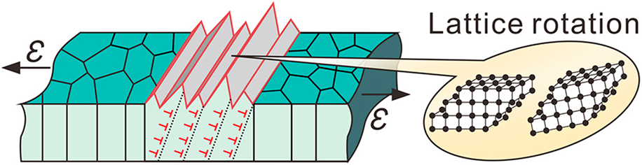
In situ atomic level studies of thermally controlled interlayer stacking shifts in 2D transition metal dichalcogenide bilayers
-
- Journal:
- Journal of Materials Research / Volume 35 / Issue 11 / 15 June 2020
- Published online by Cambridge University Press:
- 13 January 2020, pp. 1407-1416
- Print publication:
- 15 June 2020
-
- Article
- Export citation
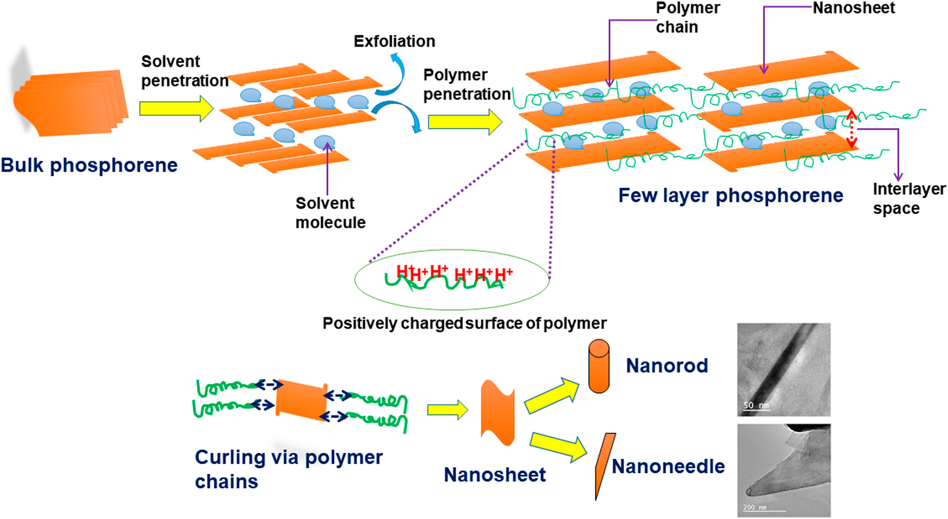
Controlled nanostructures and simultaneous passivation of black phosphorus (phosphorene) with Nafion
-
- Journal:
- Journal of Materials Research / Volume 35 / Issue 2 / 28 January 2020
- Published online by Cambridge University Press:
- 13 January 2020, pp. 141-152
- Print publication:
- 28 January 2020
-
- Article
- Export citation
Cumulative shear strain–induced preferential orientation during abnormal grain growth near fatigue crack tips of nanocrystalline Au films
-
- Journal:
- Journal of Materials Research / Volume 35 / Issue 4 / 28 February 2020
- Published online by Cambridge University Press:
- 13 January 2020, pp. 372-379
- Print publication:
- 28 February 2020
-
- Article
- Export citation
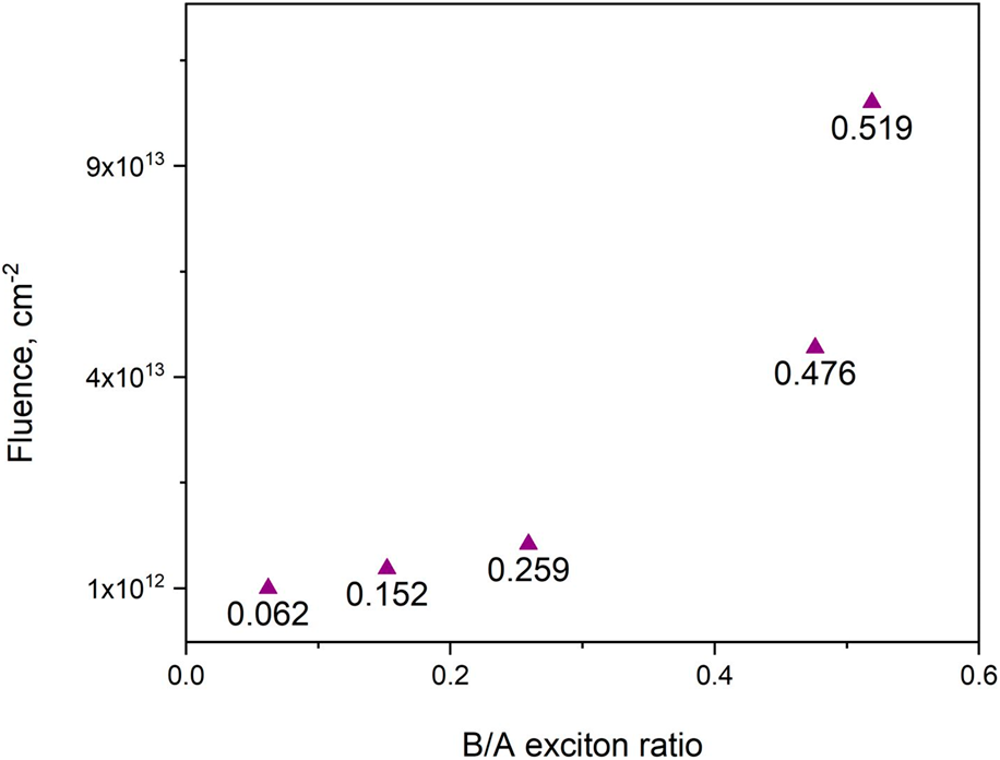
Controlling neutral and charged excitons in MoS2 with defects
-
- Journal:
- Journal of Materials Research / Volume 35 / Issue 8 / 28 April 2020
- Published online by Cambridge University Press:
- 13 January 2020, pp. 949-957
- Print publication:
- 28 April 2020
-
- Article
-
- You have access
- Open access
- HTML
- Export citation
