Refine search
Actions for selected content:
106116 results in Materials Science

Energy materials for transient power sources
-
- Journal:
- MRS Bulletin / Volume 45 / Issue 2 / February 2020
- Published online by Cambridge University Press:
- 10 February 2020, pp. 121-128
- Print publication:
- February 2020
-
- Article
- Export citation
Advanced manufacturing for transient electronics
-
- Journal:
- MRS Bulletin / Volume 45 / Issue 2 / February 2020
- Published online by Cambridge University Press:
- 10 February 2020, pp. 113-120
- Print publication:
- February 2020
-
- Article
- Export citation
MRS Journal Highlights
-
- Journal:
- MRS Bulletin / Volume 45 / Issue 2 / February 2020
- Published online by Cambridge University Press:
- 10 February 2020, p. 142
- Print publication:
- February 2020
-
- Article
-
- You have access
- HTML
- Export citation
The emergence of transient electronic devices
-
- Journal:
- MRS Bulletin / Volume 45 / Issue 2 / February 2020
- Published online by Cambridge University Press:
- 10 February 2020, pp. 87-95
- Print publication:
- February 2020
-
- Article
-
- You have access
- HTML
- Export citation
MRS volume 45 issue 2 Cover and Back matter
-
- Journal:
- MRS Bulletin / Volume 45 / Issue 2 / February 2020
- Published online by Cambridge University Press:
- 10 February 2020, pp. b1-b2
- Print publication:
- February 2020
-
- Article
-
- You have access
- Export citation
MRS Bulletin Volume Organizers guide technical theme topics for 2021
-
- Journal:
- MRS Bulletin / Volume 45 / Issue 2 / February 2020
- Published online by Cambridge University Press:
- 10 February 2020, p. 148
- Print publication:
- February 2020
-
- Article
-
- You have access
- HTML
- Export citation
Self-assembly of functional nanoscale materials
-
- Journal:
- MRS Bulletin / Volume 45 / Issue 2 / February 2020
- Published online by Cambridge University Press:
- 10 February 2020, pp. 135-141
- Print publication:
- February 2020
-
- Article
- Export citation
Inorganic materials for transient electronics in biomedical applications
-
- Journal:
- MRS Bulletin / Volume 45 / Issue 2 / February 2020
- Published online by Cambridge University Press:
- 10 February 2020, pp. 103-112
- Print publication:
- February 2020
-
- Article
- Export citation
LOOK AGAIN
-
- Journal:
- MRS Bulletin / Volume 45 / Issue 2 / February 2020
- Published online by Cambridge University Press:
- 10 February 2020, p. 152
- Print publication:
- February 2020
-
- Article
-
- You have access
- HTML
- Export citation

Material strategies for on-demand smart transient electronics
-
- Journal:
- MRS Bulletin / Volume 45 / Issue 2 / February 2020
- Published online by Cambridge University Press:
- 10 February 2020, pp. 129-134
- Print publication:
- February 2020
-
- Article
- Export citation
Exploring user facilities
-
- Journal:
- MRS Bulletin / Volume 45 / Issue 2 / February 2020
- Published online by Cambridge University Press:
- 10 February 2020, pp. 146-147
- Print publication:
- February 2020
-
- Article
-
- You have access
- HTML
- Export citation
Certification of Standard Reference Material 660c for powder diffraction
-
- Journal:
- Powder Diffraction / Volume 35 / Issue 1 / March 2020
- Published online by Cambridge University Press:
- 31 January 2020, pp. 17-22
-
- Article
- Export citation

Tuning surface texture of electrospun polycaprolactone fibers: Effects of solvent systems and relative humidity
-
- Journal:
- Journal of Materials Research / Volume 35 / Issue 3 / 14 February 2020
- Published online by Cambridge University Press:
- 31 January 2020, pp. 332-342
- Print publication:
- 14 February 2020
-
- Article
- Export citation
Characterization and Rietveld refinements of new dense ceramics Ba3−xSrxTb3−xCexO9 (x = 1 and 1.5) perovskites
-
- Journal:
- Powder Diffraction / Volume 35 / Issue 1 / March 2020
- Published online by Cambridge University Press:
- 31 January 2020, pp. 23-30
-
- Article
- Export citation
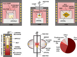
(K,Na)NbO3-based piezoelectric single crystals: Growth methods, properties, and applications
-
- Journal:
- Journal of Materials Research / Volume 35 / Issue 8 / 28 April 2020
- Published online by Cambridge University Press:
- 31 January 2020, pp. 990-1016
- Print publication:
- 28 April 2020
-
- Article
-
- You have access
- Open access
- HTML
- Export citation

Van der Waals epitaxy and composition control of layered SnSxSe2−x alloy thin films
-
- Journal:
- Journal of Materials Research / Volume 35 / Issue 11 / 15 June 2020
- Published online by Cambridge University Press:
- 31 January 2020, pp. 1386-1396
- Print publication:
- 15 June 2020
-
- Article
- Export citation
-
Epitaxial SnSxSe2−x films with tunable band gap energies (1.0–2.2 eV) are of growing interest for photodetectors and 2D heterostructures for nanoscale electronics. In this study, powder vapor transport growth of SnSxSe2−x was investigated on c-plane sapphire and epitaxial graphene (EG)/6H–SiC substrates using tin, sulfur, and selenium powder sources in a heated tube furnace. The SnSxSe2−x composition was controlled by varying the sulfur and selenium source temperatures and the corresponding chalcogen vapor pressure ratio. Raman spectroscopy was used to determine the alloy composition of the films, and the optical properties were characterized using UV-Vis-NIR spectroscopy. SnSxSe2−x grown on sapphire consisted of vertically oriented platelets. By contrast, large-area, planar coalesced SnSxSe2−x films grew on EG with low surface roughness indicative of a van der Waals growth mode. High-resolution X-ray diffraction θ–2θ scans and pole figure analysis confirm that the SnSxSe2−x films are c-axis oriented with epitaxial relation being $\left[ {11\bar{2}0} \right]$ SnSxSe2−x‖ $\left[ {10\bar{1}0} \right]$ 6H–SiC.


Electrochemical reduction of CO2 to formic acid on Bi2O2CO3/carbon fiber electrodes
-
- Journal:
- Journal of Materials Research / Volume 35 / Issue 3 / 14 February 2020
- Published online by Cambridge University Press:
- 31 January 2020, pp. 272-280
- Print publication:
- 14 February 2020
-
- Article
- Export citation
7 - Quantum Hall Effects in Graphene
-
- Book:
- Introduction to Graphene-Based Nanomaterials
- Published online:
- 10 January 2020
- Print publication:
- 30 January 2020, pp 210-236
-
- Chapter
- Export citation
2 - Electronic Properties of Carbon-Based Nanostructures
-
- Book:
- Introduction to Graphene-Based Nanomaterials
- Published online:
- 10 January 2020
- Print publication:
- 30 January 2020, pp 11-69
-
- Chapter
- Export citation
Frontmatter
-
- Book:
- Introduction to Graphene-Based Nanomaterials
- Published online:
- 10 January 2020
- Print publication:
- 30 January 2020, pp i-iv
-
- Chapter
- Export citation
