Refine search
Actions for selected content:
106116 results in Materials Science
Hot topics provide value to MRS membership and the materials community
-
- Journal:
- MRS Bulletin / Volume 45 / Issue 3 / March 2020
- Published online by Cambridge University Press:
- 11 March 2020, pp. 157-158
- Print publication:
- March 2020
-
- Article
-
- You have access
- HTML
- Export citation
EU companies increased R&D investment in 2019
-
- Journal:
- MRS Bulletin / Volume 45 / Issue 3 / March 2020
- Published online by Cambridge University Press:
- 11 March 2020, p. 169
- Print publication:
- March 2020
-
- Article
-
- You have access
- HTML
- Export citation
MRS volume 45 issue 3 Cover and Front matter
-
- Journal:
- MRS Bulletin / Volume 45 / Issue 3 / March 2020
- Published online by Cambridge University Press:
- 11 March 2020, pp. f1-f6
- Print publication:
- March 2020
-
- Article
-
- You have access
- Export citation
My constant companions
-
- Journal:
- MRS Bulletin / Volume 45 / Issue 3 / March 2020
- Published online by Cambridge University Press:
- 11 March 2020, p. 248
- Print publication:
- March 2020
-
- Article
-
- You have access
- HTML
- Export citation

Metasurface optics for imaging applications
-
- Journal:
- MRS Bulletin / Volume 45 / Issue 3 / March 2020
- Published online by Cambridge University Press:
- 11 March 2020, pp. 202-209
- Print publication:
- March 2020
-
- Article
- Export citation
Shifting the energy paradigm
-
- Journal:
- MRS Bulletin / Volume 45 / Issue 3 / March 2020
- Published online by Cambridge University Press:
- 11 March 2020, p. 175
- Print publication:
- March 2020
-
- Article
-
- You have access
- HTML
- Export citation
MRC volume 10 issue 1 Cover and Back matter
-
- Journal:
- MRS Communications / Volume 10 / Issue 1 / March 2020
- Published online by Cambridge University Press:
- 02 April 2020, pp. b1-b2
- Print publication:
- March 2020
-
- Article
-
- You have access
- Export citation
MRS volume 45 issue 3 Cover and Back matter
-
- Journal:
- MRS Bulletin / Volume 45 / Issue 3 / March 2020
- Published online by Cambridge University Press:
- 11 March 2020, pp. b1-b2
- Print publication:
- March 2020
-
- Article
-
- You have access
- Export citation
Hybrid device captures and stores solar thermal energy with high efficiency
-
- Journal:
- MRS Bulletin / Volume 45 / Issue 3 / March 2020
- Published online by Cambridge University Press:
- 11 March 2020, p. 166
- Print publication:
- March 2020
-
- Article
-
- You have access
- HTML
- Export citation
Gone with the wind: The life and death of a wind turbine rotor blade
-
- Journal:
- MRS Bulletin / Volume 45 / Issue 3 / March 2020
- Published online by Cambridge University Press:
- 11 March 2020, pp. 178-179
- Print publication:
- March 2020
-
- Article
-
- You have access
- HTML
- Export citation

Super high-dielectric-constant oxide films for next-generation nanoelectronics and supercapacitors for energy storage
-
- Journal:
- MRS Bulletin / Volume 45 / Issue 3 / March 2020
- Published online by Cambridge University Press:
- 11 March 2020, pp. 231-238
- Print publication:
- March 2020
-
- Article
- Export citation
Preview: 2020 Materials Research Society Spring Meeting & Exhibit
-
- Journal:
- MRS Bulletin / Volume 45 / Issue 3 / March 2020
- Published online by Cambridge University Press:
- 11 March 2020, pp. 240-245
- Print publication:
- March 2020
-
- Article
-
- You have access
- HTML
- Export citation

Transdimensional material platforms for tunable metasurface design
-
- Journal:
- MRS Bulletin / Volume 45 / Issue 3 / March 2020
- Published online by Cambridge University Press:
- 11 March 2020, pp. 188-195
- Print publication:
- March 2020
-
- Article
- Export citation
JMR volume 35 issue 4 Cover and Back matter
-
- Journal:
- Journal of Materials Research / Volume 35 / Issue 4 / 28 February 2020
- Published online by Cambridge University Press:
- 28 February 2020, pp. b1-b5
- Print publication:
- 28 February 2020
-
- Article
-
- You have access
- Export citation
JMR volume 35 issue 4 Cover and Front matter
-
- Journal:
- Journal of Materials Research / Volume 35 / Issue 4 / 28 February 2020
- Published online by Cambridge University Press:
- 28 February 2020, pp. f1-f4
- Print publication:
- 28 February 2020
-
- Article
-
- You have access
- Export citation

A brief review of data-driven ICME for intelligently discovering advanced structural metal materials: Insight into atomic and electronic building blocks
-
- Journal:
- Journal of Materials Research / Volume 35 / Issue 8 / 28 April 2020
- Published online by Cambridge University Press:
- 28 February 2020, pp. 872-889
- Print publication:
- 28 April 2020
-
- Article
-
- You have access
- Open access
- HTML
- Export citation

Influence of microstructure degradation induced by pretreatment on the creep behavior in Ni-based single-crystal superalloy with different orientations
-
- Journal:
- Journal of Materials Research / Volume 35 / Issue 6 / 30 March 2020
- Published online by Cambridge University Press:
- 26 February 2020, pp. 610-622
- Print publication:
- 30 March 2020
-
- Article
- Export citation
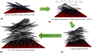
Highly stable multi-layered silicon-intercalated graphene anodes for lithium-ion batteries
-
- Journal:
- MRS Communications / Volume 10 / Issue 1 / March 2020
- Published online by Cambridge University Press:
- 26 February 2020, pp. 25-31
- Print publication:
- March 2020
-
- Article
- Export citation
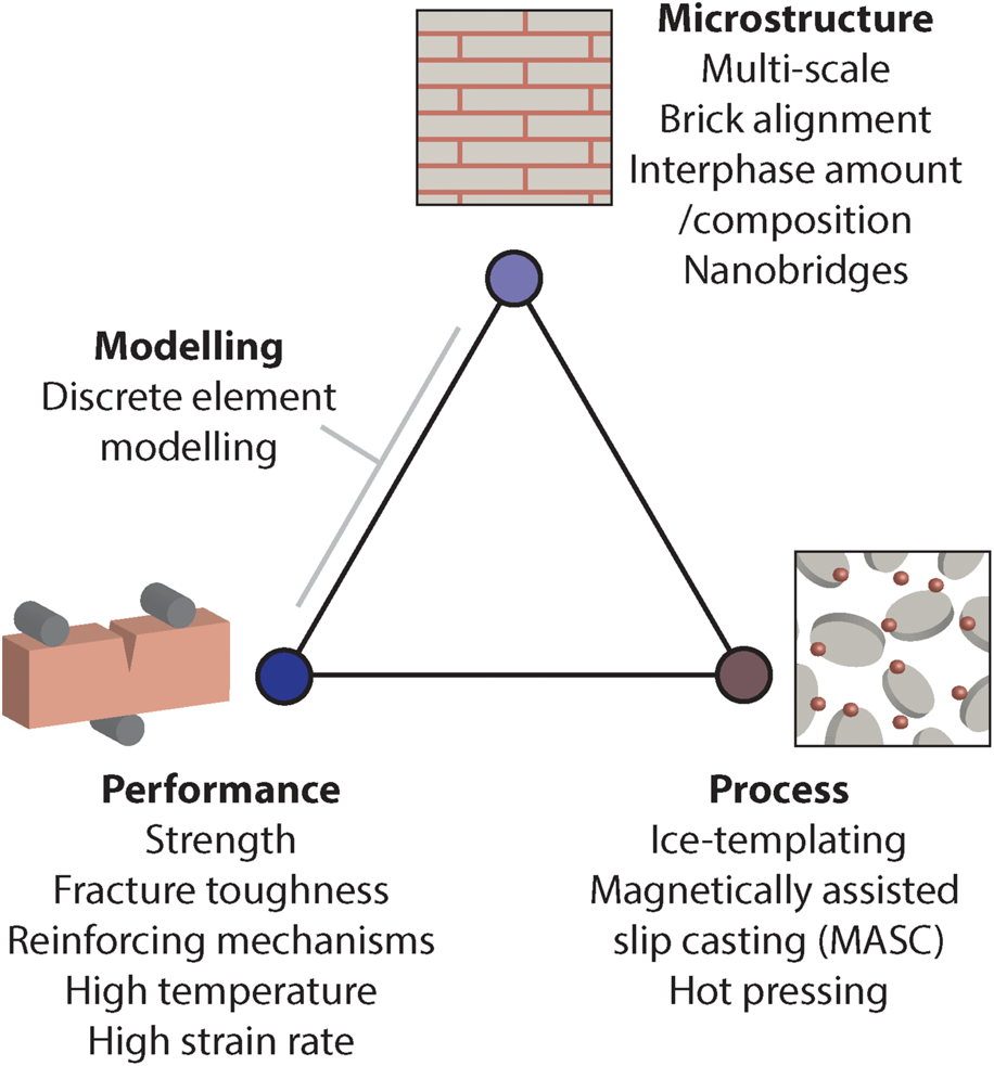
Strong and tough nacre-like aluminas: Process–structure–performance relationships and position within the nacre-inspired composite landscape
-
- Journal:
- Journal of Materials Research / Volume 35 / Issue 8 / 28 April 2020
- Published online by Cambridge University Press:
- 24 February 2020, pp. 1076-1094
- Print publication:
- 28 April 2020
-
- Article
-
- You have access
- Open access
- HTML
- Export citation
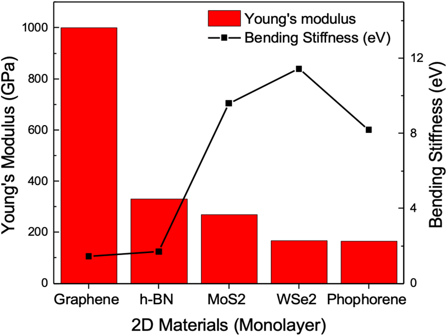
Heterogeneous deformation of two-dimensional materials for emerging functionalities
-
- Journal:
- Journal of Materials Research / Volume 35 / Issue 11 / 15 June 2020
- Published online by Cambridge University Press:
- 24 February 2020, pp. 1369-1385
- Print publication:
- 15 June 2020
-
- Article
- Export citation
