Refine search
Actions for selected content:
106116 results in Materials Science

Study on the band gap optimization and defect state of two-dimensional honeycomb phononic crystals
-
- Journal:
- Journal of Materials Research / Volume 35 / Issue 21 / 16 November 2020
- Published online by Cambridge University Press:
- 10 September 2020, pp. 3021-3030
- Print publication:
- 16 November 2020
-
- Article
- Export citation

Functional piezoelectric yarn: Toward optimization of zinc oxide nanowires growth
-
- Journal:
- Journal of Materials Research / Volume 35 / Issue 22 / 30 November 2020
- Published online by Cambridge University Press:
- 10 September 2020, pp. 3091-3105
- Print publication:
- 30 November 2020
-
- Article
- Export citation

Influence of side-chain isomerization on the isothermal crystallization kinetics of poly(3-alkylthiophenes)
-
- Journal:
- Journal of Materials Research , First View
- Published online by Cambridge University Press:
- 07 September 2020, pp. 1-12
-
- Article
- Export citation
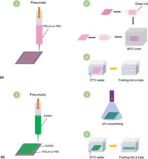
3D Printed porous tissue engineering scaffolds with the self-folding ability and controlled release of growth factor
-
- Journal:
- MRS Communications / Volume 10 / Issue 4 / December 2020
- Published online by Cambridge University Press:
- 04 September 2020, pp. 579-586
- Print publication:
- December 2020
-
- Article
- Export citation

In situ silver nanoparticle synthesis on 3D-printed polylactic acid scaffolds for biomedical applications
-
- Journal:
- Journal of Materials Research , First View
- Published online by Cambridge University Press:
- 03 September 2020, pp. 1-10
-
- Article
- Export citation

Calcia–magnesia–alumina-silica particle deposition prediction in gas turbines using a Eulerian–Lagrangian approach in computational fluid dynamics
-
- Journal:
- Journal of Materials Research / Volume 35 / Issue 17 / 14 September 2020
- Published online by Cambridge University Press:
- 03 September 2020, pp. 2288-2299
- Print publication:
- 14 September 2020
-
- Article
- Export citation
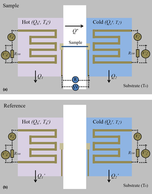
MEMS-based dual temperature control measurement method for thermoelectric properties of individual nanowires
-
- Journal:
- MRS Communications / Volume 10 / Issue 4 / December 2020
- Published online by Cambridge University Press:
- 03 September 2020, pp. 620-627
- Print publication:
- December 2020
-
- Article
- Export citation

Thermodynamic properties of rare-earth alloys by electrochemical emf measurements
-
- Journal:
- Journal of Materials Research , First View
- Published online by Cambridge University Press:
- 03 September 2020, pp. 1-9
-
- Article
- Export citation
A legend reborn: Additive manufacturing creates Wootz-Damascus steel
-
- Journal:
- MRS Bulletin / Volume 45 / Issue 9 / September 2020
- Published online by Cambridge University Press:
- 10 September 2020, p. 685
- Print publication:
- September 2020
-
- Article
-
- You have access
- HTML
- Export citation
The COVID-19 pandemic informs future directions of US research universities
-
- Journal:
- MRS Bulletin / Volume 45 / Issue 9 / September 2020
- Published online by Cambridge University Press:
- 10 September 2020, pp. 687-693
- Print publication:
- September 2020
-
- Article
-
- You have access
- HTML
- Export citation
Nucleation, growth, and superlattice formation of nanocrystals observed in liquid cell transmission electron microscopy
-
- Journal:
- MRS Bulletin / Volume 45 / Issue 9 / September 2020
- Published online by Cambridge University Press:
- 10 September 2020, pp. 713-726
- Print publication:
- September 2020
-
- Article
- Export citation

Liquid phase electron microscopy of biological specimens
-
- Journal:
- MRS Bulletin / Volume 45 / Issue 9 / September 2020
- Published online by Cambridge University Press:
- 10 September 2020, pp. 754-760
- Print publication:
- September 2020
-
- Article
- Export citation
Mrs Movers & Shakers: Spread the good news!
-
- Journal:
- MRS Bulletin / Volume 45 / Issue 9 / September 2020
- Published online by Cambridge University Press:
- 10 September 2020, pp. 783-784
- Print publication:
- September 2020
-
- Article
-
- You have access
- HTML
- Export citation
How to define your “field of endeavor” for your EB-1A/NIW petition
-
- Journal:
- MRS Bulletin / Volume 45 / Issue 9 / September 2020
- Published online by Cambridge University Press:
- 10 September 2020, p. 782
- Print publication:
- September 2020
-
- Article
-
- You have access
- HTML
- Export citation

In situ electrochemical scanning/transmission electron microscopy of electrode–electrolyte interfaces
-
- Journal:
- MRS Bulletin / Volume 45 / Issue 9 / September 2020
- Published online by Cambridge University Press:
- 10 September 2020, pp. 738-745
- Print publication:
- September 2020
-
- Article
- Export citation
MRC volume 10 issue 3 Cover and Back matter
-
- Journal:
- MRS Communications / Volume 10 / Issue 3 / September 2020
- Published online by Cambridge University Press:
- 14 September 2020, pp. b1-b2
- Print publication:
- September 2020
-
- Article
-
- You have access
- Export citation

Electron-beam-driven chemical processes during liquid phase transmission electron microscopy
-
- Journal:
- MRS Bulletin / Volume 45 / Issue 9 / September 2020
- Published online by Cambridge University Press:
- 10 September 2020, pp. 746-753
- Print publication:
- September 2020
-
- Article
- Export citation
Materials science, energy transition, and the pandemic
-
- Journal:
- MRS Bulletin / Volume 45 / Issue 9 / September 2020
- Published online by Cambridge University Press:
- 10 September 2020, p. 697
- Print publication:
- September 2020
-
- Article
-
- You have access
- HTML
- Export citation
Takiya Ahmed Foskey Chemist and community outreach champion
-
- Journal:
- MRS Bulletin / Volume 45 / Issue 9 / September 2020
- Published online by Cambridge University Press:
- 10 September 2020, p. 781
- Print publication:
- September 2020
-
- Article
-
- You have access
- HTML
- Export citation
Liquid phase transmission electron microscopy for imaging of nanoscale processes in solution
-
- Journal:
- MRS Bulletin / Volume 45 / Issue 9 / September 2020
- Published online by Cambridge University Press:
- 10 September 2020, pp. 704-712
- Print publication:
- September 2020
-
- Article
-
- You have access
- HTML
- Export citation
