Article contents
Simultaneously grown single wall carbon nanotube channel and electrodes in a thin film transistor
Published online by Cambridge University Press: 22 June 2012
Abstract

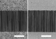
By chemical vapor deposition, aligned single wall carbon nanotubes (SWNTs) and a network of SWNTs are simultaneously grown as the channel and the source–drain electrodes of thin film transistors (TFTs). The increase of aligned SWNTs increases the channel conductance without changing the contact resistance. However, the increase of network-type SWNTs from 19 to 32.5 (SWNTs/μm) decreases the contact resistance fivefold. The contact resistance of all-SWNT TFT is three times lower compared with that of an SWNT TFT using metal electrodes. The all-SWNT TFTs transferred on polyethylene terephthalate (PET) show a transparency of >80% in the visible range of wavelengths.
- Type
- Research Letters
- Information
- Copyright
- Copyright © Materials Research Society 2012
References
- 2
- Cited by


