Hostname: page-component-745bb68f8f-g4j75 Total loading time: 0 Render date: 2025-01-14T10:07:36.626Z Has data issue: false hasContentIssue false

Resistive-nanoindentation: contact area monitoring by real-time electrical contact resistance measurement

Published online by Cambridge University Press:  07 June 2019

Solène Comby-Dassonneville
Affiliation:
Univ. Grenoble Alpes, CNRS, Grenoble INP, SIMaP, 38000 Grenoble, France
Fabien Volpi*
Affiliation:
Univ. Grenoble Alpes, CNRS, Grenoble INP, SIMaP, 38000 Grenoble, France
Guillaume Parry
Affiliation:
Univ. Grenoble Alpes, CNRS, Grenoble INP, SIMaP, 38000 Grenoble, France
Didier Pellerin
Affiliation:
Scientec/CSInstruments, 91940 Les Ulis, France
Marc Verdier
Affiliation:
Univ. Grenoble Alpes, CNRS, Grenoble INP, SIMaP, 38000 Grenoble, France
*
Address all correspondence to Fabien Volpi at fabien.volpi@simap.grenoble-inp.fr
Get access

Abstract

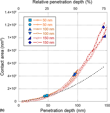
In the past decades, efforts have been made to couple nanoindentation with resistive measurements in order to monitor the real-time contact area, as an alternative to the use of traditional analytical models. In this work, a novel and efficient stand-alone method is proposed to compute the contact area using resistive-nanoindentation of noble metals (bulk or thin films). This method relies on three steps: tip shape measurement, set-up calibration, application to the sample to be characterized. The procedure is applied to nanoindentation tests on a sample with film-on-elastic-substrate rheology and is successfully validated against experimental measurements of the contact area.

Type
Research Letters
Copyright
Copyright © Materials Research Society 2019 

Access options

Get access to the full version of this content by using one of the access options below. (Log in options will check for institutional or personal access. Content may require purchase if you do not have access.)

References

1.Nili, H., Kalantar-Zadeh, K., Bhaskaran, M., and Sriram, S.: In situ nanoindentation: probing nanoscale multifunctionality. Prog. Mater. Sci. 58, 1 (2013) https://doi.org/10.1016/j.pmatsci.2012.08.001.Google Scholar
2.Clarke, D.R., Kroll, M., Kirchner, P.D., Cook, R.F., and Hockey, B.J.: Amorphization and conductivity of silicon and germanium induced by indentation. Phys. Rev. Lett. 60, 2156 (1988) https://doi.org/10.1103/PhysRevLett.60.2156.Google Scholar
3.Pharr, G.M., Oliver, W.C., Cook, R.F., Kirchner, P.D., Kroll, M., and Dinger, T.R.: Electrical resistance of metallic contacts on silicon and germanium during indentation. J. Mater. Res. 7, 961 (1992) https://doi.org/10.1557/JMR.1992.0961.Google Scholar
4.Mann, A.B., van Heerden, D., Pethica, J.B., and Weihs, T.P.: Size-dependent phase transformation during point loading of silicon. J. Mater. Res. 15, 1754 (2000) https://doi.org/10.1557/JMR.2000.0253.Google Scholar
5.Mann, A.B., van Heerden, D., Pethica, J.B., Bowes, P., and Weihs, T.P.: Contact resistance and phase transformation during nanoindentation of silicon. Philos. Mag. A 82, 1921 (2002) https://doi.org/10.1080/01418610208235704.Google Scholar
6.Bradby, J.E., Williams, J.S., and Swain, M.V.: In situ electrical characterisation of phase transformation in Si during indentation. Phys. Rev. 67, 085205 (2003) https://doi.org/10.1103/PhysRevB.67.085205.Google Scholar
7.Ruffell, S., Bradby, J.E., Williams, J.S., and Warren, O.L.: An in situ electrical measurement technique via a conducting diamond tip for nanoindentation in silicon. J. Mater. Res. 22, 578 (2007) https://doi.org/10.1557/jmr.2007.0100.Google Scholar
8.Ruffell, S., Bradby, J.E., Fujisawa, N., and Williams, J.S.: Identification of nanoindentation-induced phase changes in silicon by in situ electrical characterization. J. Appl. Phys. 101, 083531 (2007) https://doi.org/10.1063/1.2724803.Google Scholar
9.Pethica, J.B. and Tabor, D.: Contact of characterised metal surface at very low loads: deformation and adhesion. Surf. Sci. 89, 189 (1979) https://doi.org/10.1016/0039-6028(79)90606-X.Google Scholar
10.Stauffer, D.D., Major, R.C., Vodnick, D., Thomas, J.H., Parkern, J., Manno, M., Leighton, C., and Gerberich, W.W.: Plastic response of the native oxide on Cr and Al thin films from in situ conductive nanoindentation. J. Mater. Res. 27, 685 (2012) https://doi.org/10.1557/jmr.2011.432.Google Scholar
11.Nguyen, H.H., Wei, P.J., and Lin, J.F.: Electrical contact resistance for monitoring nanoindentation-induced delamination. Adv. Nat. Sci.: Nanosci. Nanotechnol. 2, 015007 (2011) https://doi.org/10.1088/2043-6262/2/1/015007.Google Scholar
12.Duvivier, P.Y., Mandrillon, V., Inal, K., Dieppedale, C., Deldon-Martoscia, S., and Polizzi, J.P.: Time dependence investigation of the electrical resistance of Au/Au thin film micro contacts. Proc. 56th IEEE Holm Conf. Elect. Cont. 58 (2010) https://doi.org/10.1109/HOLM.2010.5619563.Google Scholar
13.Arrazat, B., Duvivier, P.Y., Mandrillon, V., and Inal, K.: Discrete analysis of gold surface asperities deformation under spherical nano-indentation towards electrical contact resistance calculation. Proc. 57th IEEE Holm Conf. Elect. Cont. 1, (2011) https://doi.org/10.1109/HOLM.2011.6034798.Google Scholar
14.Fang, L., Muhlstein, C.L., Collins, J.G., Romasco, A.L., and Friedman, L.H.: Continuous electrical in situ contact area measurement during instrumented indentation. J. Mater. Res. 23, 2480 (2008) https://doi.org/10.1557/jmr.2008.0298.Google Scholar
15.Sprouster, D.J., Ruffel, S., Bradby, J.E., Stauffer, D.D. and Major, R.C., Warren, O.L., and Williams, J.S.: Quantitative electromechanical characterization of materials using conductive ceramic tips. Acta Mater. 71, 153 (2014) https://doi.org/10.1016/j.actamat.2014.02.028.Google Scholar
16.Sneddon, I.N.: The relation between load and penetration in the axisymmetric boussinesq problem for a punch of arbitrary profile. Int. J. Eng. Sci., 3, 47 (1965) https://doi.org/10.1016/0020-7225(65)90019-4.Google Scholar
17.Oliver, W.C. and Pharr, G.M.: Measurements of hardness and elastic modulus by instrumented indentation: advances in understanding and refinements to methodology. J. Mater. Res. 19, 3 (2004) http://dx.doi.org/10.1557/jmr.2004.0002.Google Scholar
18.Oliver, W.C. and Pharr, G.M.: An improved technique for determining hardness and elastic modulus using load and displacement sensing indentation experiments. J. Mater. Res. 7, 1564 (1992) https://doi.org/10.1557/JMR.1992.1564.Google Scholar
19.Loubet, J.L., Bauer, M., Tonck, A., Bec, S., and Gauthier-Manuel, B.: Mechanical properties and deformation behavior of materials having ultra-fine microstructures: nanoexperiments with a surface force apparatus. In Mechanical Properties and Deformation Behavior of Materials Having Ultra-Fine Microstructures, edited by Nastasi, M., Parkin, D.M. and Gleiter, H. (Springer Netherlands, Dordrecht 429, 1993) https://doi.org/10.1007/978-94-011-1765-4.Google Scholar
20.Houzé, F., Meyer, R., Schneegans, O., and Boyer, L.: Imaging the local electrical properties of metal surfaces by atomic force microscopy with conducting probes. Appl. Phys. Lett. 69, 1975 (1996) https://doi.org/10.1063/1.117179.Google Scholar
21.Gwyddion software. Available at: http://gwyddion.net/download.php (accessed 14 May 2019).Google Scholar
22.Charleux, L., Keryvin, V., Nivard, M., Guin, J.-P., Sangleboeuf, J.-C., and Yokoyama, Y.: A method for measuring the contact area in instrumented indentation testing by tip scanning probe microscopy imaging, Acta Mat. 70, 249258 (2014) https://doi.org/10.1016/j.actamat.2014.02.036.Google Scholar
23.Schneegans, O., Chrétien, P., Houzé, F., and Meyer, R.: Capacitance measurements on small parallel plate capacitors using nanoscale impedance microscopy. Appl. Phys. Lett. 90, 043116 (2007) https://doi.org/10.1063/1.2437052.Google Scholar
24.Romano, J.D. and Price, R.H.: The conical resistor conundrum: a potential solution. Am. J. Phys., 64, 1150 (1996) https://doi.org/10.1119/1.18335.Google Scholar
25.Nakamura, M.: Constriction resistance of conducting spots by the boundary element method. IEEE Trans. Comp. Hybrids, Manufact. Technol. 16, 339 (1993) https://doi.org/10.1109/33.232062.Google Scholar
26.Sharvin, Y.: A possible method for studying Fermi surfaces. Sov. Phys. JETP 21, 655 (1965).Google Scholar
27.Greenwood, J.A.: Constriction resistance and the real area of contact. J. Appl. Phys. 17, 1621 (1966) https://doi.org/10.1088/0508-3443/17/12/310.Google Scholar
28.Perriot, A. and Barthel, E.: Elastic contact to a coated half-space-effective elastic modulus and real penetration. J. Mater. Res. 19, 600 (2004) https://doi.org/10.1557/jmr.2004.19.2.600.Google Scholar
Supplementary material: File

Comby-Dassonneville et al. supplementary material

Comby-Dassonneville et al. supplementary material 1

Download Comby-Dassonneville et al. supplementary material(File)
File 171 KB