Hostname: page-component-745bb68f8f-cphqk Total loading time: 0 Render date: 2025-01-14T10:45:01.379Z Has data issue: false hasContentIssue false

A pathway to compound semiconductor additive manufacturing

Published online by Cambridge University Press:  27 August 2019

Jarod C. Gagnon*
Affiliation:
Johns Hopkins University Applied Physics Laboratory, 11100 Johns Hopkins Rd., Laurel, MD 20723, USA
Michael Presley
Affiliation:
Johns Hopkins University Applied Physics Laboratory, 11100 Johns Hopkins Rd., Laurel, MD 20723, USA
Nam Q. Le
Affiliation:
Johns Hopkins University Applied Physics Laboratory, 11100 Johns Hopkins Rd., Laurel, MD 20723, USA
Timothy J. Montalbano
Affiliation:
Johns Hopkins University Applied Physics Laboratory, 11100 Johns Hopkins Rd., Laurel, MD 20723, USA
Steven Storck
Affiliation:
Johns Hopkins University Applied Physics Laboratory, 11100 Johns Hopkins Rd., Laurel, MD 20723, USA
*
Address all correspondence to Jarod C. Gagnon at Jarod.Gagnon@jhuapl.edu
Get access

Abstract

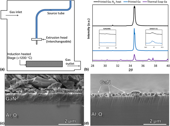
The rise of additive manufacturing (AM) has enabled the rapid production of complex part geometries across multiple material domains. To date, however, AM of inorganic semiconductor materials has not been fully realized due to the difficulty of forming single-crystal materials with traditional AM processes. Here, we demonstrate a novel semiconductor synthesis method using a combination of liquid and gas precursors to additively print gallium nitride. Growth rates of 1–2 µm/min are demonstrated in printed regions while maintaining epitaxial alignment with the substrate. We also outline critical variables for the future development, improvement, and implementation of the proposed process.

Type
Research Letters
Copyright
Copyright © The Author(s) 2019 

Access options

Get access to the full version of this content by using one of the access options below. (Log in options will check for institutional or personal access. Content may require purchase if you do not have access.)

References

1.Bourell, D.L., Rosen, D.W., and Leu, M.C.: The roadmap for additive manufacturing and its impact. 3D Print. Addit. Manuf. 1, 69 (2014).10.1089/3dp.2013.0002Google Scholar
2.Huang, S.H., Liu, P., Mokasdar, A., and Hou, L.: Additive manufacturing and its societal impact: a literature review. Int. J. Adv. Manuf. Technol. 67, 11911203 (2013).10.1007/s00170-012-4558-5Google Scholar
3.Ngo, T.D., Kashani, A., Imbalzano, G., Nguyen, K.T.Q., and Hui, D.: Additive manufacturing (3D printing): a review of materials, methods, applications and challenges. Compos. Part B Eng. 143, 172196 (2018).10.1016/j.compositesb.2018.02.012Google Scholar
4.Fortunato, E., Barquinha, P., and Martins, R.: Oxide semiconductor thin-film transistors: a review of recent advances. Adv. Mater. 24, 29452986 (2012).10.1002/adma.201103228Google Scholar
5.Morkoç, H., Strite, S., Gao, G.B., Lin, M.E., Sverdlov, B., and Burns, M.: Large-band-gap SiC, III-V nitride, and II-VI ZnSe-based semiconductor device technologies. J. Appl. Phys. 76, 13631398 (1994).Google Scholar
6.Chow, T.P. and Tyagi, R.: Wide bandgap compound semiconductors for superior high-voltage unipolar power devices. IEEE Trans. Electron. Devices 41, 14811483 (1994).10.1109/16.297751Google Scholar
7.Kizilyalli, I.C., Edwards, A.P., Aktas, O., Prunty, T., and Bour, D.: Vertical power p-n diodes based on bulk GaN. IEEE Trans. Electron. Devices 62, 414422 (2015).10.1109/TED.2014.2360861Google Scholar
8.Saengchairat, N., Tuan, T., and Chee-Kai, C.: A review: additive manufacturing for active electronic components. Virtual Phys. Prototyping 12, 3146 (2017).Google Scholar
9.Wei, H.L., Mazumder, J., and DebRoy, T.: Evolution of solidification texture during additive manufacturing. Sci. Rep. 5, 16446 (2015).10.1038/srep16446Google Scholar
10.Rödel, J., Kounga, A.B.N, Weissenberger-Eibl, M., Koch, D., Bierwisch, A., Rossner, W., Hoffmann, M.J., Danzer, R., and Schneider, G.: Development of a roadmap for advanced ceramics: 2010–2025. J. Eur. Ceram. Soc. 29, 15491560 (2009).10.1016/j.jeurceramsoc.2008.10.015Google Scholar
11.Klemenz, C. and Scheel, H.J.: Crystal growth and liquid-phase epitaxy of gallium nitride. J. Cryst. Growth 211 6267 (2000).10.1016/S0022-0248(99)00831-3Google Scholar
12.Azizi, M., Meissner, E., Friedrich, J., and Muller, G.: Liquid phase epitaxy (LPE) of GaN on c- and r-faces of AlN substrates. J. Cryst. Growth 322, 7477 (2011).10.1016/j.jcrysgro.2011.03.014Google Scholar
13.Dickey, M.D.: Emerging applications of liquid metals featuring surface oxides. ACS Appl. Mater. Interface 6, 1836918379 (2014).Google Scholar
14.Ladd, C., So, J.H., Muth, J., and Dickey, M.D.: 3D printing of free standing liquid metal microstructures. Adv. Mater. 25, 50815085 (2013).10.1002/adma.201301400Google Scholar
15.Logan, R.A. and Thurmond, C.D.: Heteroepitaxial thermal gradient solution growth of GaN. J. Electrochem. Soc. Solid-State Sci. Technol. 119, 17271735 (1972).Google Scholar
16.Klinedinst, K.A. and Stevenson, D.A.: Oxygen diffusion in liquid gallium and indium. J. Electrochem. Soc. 120, 304308 (1973).Google Scholar
17.Liu, Y., Long, Z., Wang, H., Du, Y., and Huang, B.: A predictive equation for solute diffusivity in liquid metals. Scr. Mater. 55, 367370 (2006).10.1016/j.scriptamat.2006.04.019Google Scholar
18.Unland, J., Onderka, B., Davydov, A., and Schmid-Fetzer, R.: Thermodynamics and phase stability in the Ga-N system. J. Cryst. Growth 256, 3351 (2003).Google Scholar
19.Garcia, R., Ren, B., Thomas, A.C., and Ponce, F.A.: Measurement of the solubility of ammonia and nitrogen in gallium at atmospheric pressure. J. Alloys Comp. 467, 611613 (2009).10.1016/j.jallcom.2008.03.075Google Scholar
20.Ambacher, O.: Growth and applications of group III-nitrides. J. Appl. Phys. D Appl. Phys. 31, 26532710 (1998).10.1088/0022-3727/31/20/001Google Scholar
21.Tanaka, A., Funayama, Y., Murakami, T., and Katsuno, H.: GaN crystal growth on an SiC substrate from Ga wetting solution reacting with NH3. J. Cryst. Growth 249, 5964 (2003).10.1016/S0022-0248(02)02097-3Google Scholar