Hostname: page-component-745bb68f8f-lrblm Total loading time: 0 Render date: 2025-01-27T23:25:38.842Z Has data issue: false hasContentIssue false

Highly strained Ge micro-blocks bonded on Si platform for mid-infrared photonic applications

Published online by Cambridge University Press:  10 July 2017

A. Gassenq*
Affiliation:
Univ. Grenoble Alpes, CEA, INAC, PHELIQS, F-38000 Grenoble, France
K. Guilloy
Affiliation:
Univ. Grenoble Alpes, CEA, INAC, PHELIQS, F-38000 Grenoble, France
N. Pauc
Affiliation:
Univ. Grenoble Alpes, CEA, INAC, PHELIQS, F-38000 Grenoble, France
D. Rouchon
Affiliation:
CEA-LETI, Univ. Grenoble Alpes, 38000 Grenoble, France
J. Widiez
Affiliation:
CEA-LETI, Univ. Grenoble Alpes, 38000 Grenoble, France
J. Rothman
Affiliation:
CEA-LETI, Univ. Grenoble Alpes, 38000 Grenoble, France
J.-M. Hartmann
Affiliation:
CEA-LETI, Univ. Grenoble Alpes, 38000 Grenoble, France
A. Chelnokov
Affiliation:
CEA-LETI, Univ. Grenoble Alpes, 38000 Grenoble, France
V. Reboud
Affiliation:
CEA-LETI, Univ. Grenoble Alpes, 38000 Grenoble, France
V. Calvo
Affiliation:
Univ. Grenoble Alpes, CEA, INAC, PHELIQS, F-38000 Grenoble, France
*
Address all correspondence to A. Gassenq at albangassenq@yahoo.fr
Get access

Abstract

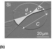
Applying sufficient tensile strain to Ge leads to a direct bandgap group IV semiconductor, which emits in the mid-infrared (MIR) wavelength range. However, highly strained-Ge cannot be directly grown on Si because of its large lattice mismatch. In this work, we have developed a process based on Ge micro-bridge strain redistribution intentionally landed to the Si substrate. Traction arms were then partially etched to keep locally strained-Ge micro-blocks. Large tunable uniaxial stresses up to 4.2% strain were demonstrated in Ge, which was bonded on Si. Our approach allows envisioning integrated strained-Ge on Si platform for MIR-integrated optics. Silicon photonics merge optical and electronic components that can be integrated together onto a single microchip.

Type
Research Letters
Copyright
Copyright © Materials Research Society 2017 

Access options

Get access to the full version of this content by using one of the access options below. (Log in options will check for institutional or personal access. Content may require purchase if you do not have access.)

References

1.Roelkens, G., Dave, U., Gassenq, A., Hattasan, N., Hu, C., Kuyken, B., Leo, F., Malik, A., Muneeb, M., Ryckeboer, E., Uvin, S., Hens, Z., Baets, R., Shimura, Y., Gencarelli, F., Vincent, B., Loo, R., Van Campenhout, J., Cerutti, L., Rodriguez, J.-B., Tournié, E., Chen, X., Nedeljkovic, M., Mashanovich, G., Shen, L., Healy, N., Peacock, A.C., Liu, X., Osgood, R., and Green, W.: Silicon-based heterogeneous photonic integrated circuits for the mid-infrared. Opt. Mater. Express 3, 1523 (2013).Google Scholar
2.Soref, R.: Mid-infrared photonics in silicon and germanium. Nat. Photonics 4, 495497 (2010).Google Scholar
3.Ryckeboer, E., Gassenq, A., Muneeb, M., Hattasan, N., Bogaerts, W., Cerutti, L., Rodriguez, J.B., and Tournié, E.: Silicon-on-insulator spectrometers with integrated GaInAsSb photodiodes for wide-band spectroscopy from 1510 to 2300 nm abstract: Opt. Express 21, 61016108 (2013).Google Scholar
4.Barritault, P., Brun, M., Labeye, P., Hartmann, J.-M., Boulila, F., Carras, M., and Nicoletti, S.: Design, fabrication and characterization of an AWG at 4.5 µm. Opt. Express 23, 26168 (2015).Google Scholar
5.Malik, A., Muneeb, M., Shimura, Y., Van Campenhout, J., Loo, R., and Roelkens, G.: Germanium-on-silicon planar concave grating wavelength (de)multiplexers in the mid-infrared. Appl. Phys. Lett. 103, 16119 (2013).Google Scholar
6.Reboul, J.R., Cerutti, L., Rodriguez, J.B., Grech, P., and Tournié, E.: Continuous-wave operation above room temperature of GaSb-based laser diodes grown on Si. Appl. Phys. Lett. 99, 20092012 (2011).Google Scholar
7.Wang, Z., Tian, B., Pantouvaki, M., Guo, W., Absil, P., Van Campenhout, J., Merckling, C., and Van Thourhout, D.: Room temperature InP DFB laser array directly grown on (001) silicon. Nat. Photonics 9, 837842 (2015).Google Scholar
8.Gassenq, A., Hattasan, N., Cerutti, L., Rodriguez, J.B., Tournié, E., and Roelkens, G.: Study of evanescently-coupled and grating-assisted GaInAsSb photodiodes integrated on a silicon photonic chip. Opt. Express 20, 11665 (2012).Google Scholar
9.Wang, R., Sprengel, S., Muneeb, M., Boehm, G., Baets, R., Amann, M.-C., and Roelkens, G.: 2 µm wavelength range InP-based type-II quantum well photodiodes heterogeneously integrated on silicon photonic integrated circuits. Opt. Express 23, 26834 (2015).Google Scholar
10.Liu, J., Sun, X., Camacho-Aguilera, R., Kimerling, L.C., and Michel, J.: Ge-on-Si laser operating at room temperature. Opt. Lett. 35, 679 (2010).Google Scholar
11.Wirths, S., Geiger, R., von den Driesch, N., Mussler, G., Stoica, T., Mantl, S., Ikonic, Z., Luysberg, M., Chiussi, S., Hartmann, J.M., Sigg, H., Faist, J., Buca, D., and Grützmacher, D.: Lasing in direct-bandgap GeSn alloy grown on Si. Nat. Photonics 9, 88 (2015).Google Scholar
12.Gassenq, A., Gencarelli, F., Van Campenhout, J., Shimura, Y., Loo, R., Narcy, G., Vincent, B., and Roelkens, G.: GeSn/Ge heterostructure short-wave infrared photodetectors on silicon. Opt. Express 20, 2729727303 (2012).Google Scholar
13.Pham, T., Du, W., Tran, H., Margetis, J., Tolle, J., Sun, G., Soref, R.A., Naseem, H.A., Li, B., and Yu, S.-Q.: Systematic study of Si-based GeSn photodiodes with 2.6 µm detector cutoff for short-wave infrared detection. Opt. Express 24, 4519 (2016).Google Scholar
14.Geiger, R., Zabel, T., Marin, E., Gassenq, A., Hartmann, J.-M., Widiez, J., Escalante, J., Guilloy, K., Pauc, N., Rouchon, D., Diaz, G.O., Tardif, S., Rieutord, F., Duchemin, I., Niquet, Y.-M., Reboud, V., Calvo, V., Chelnokov, A., Faist, J., and Sigg, H.: Uniaxially stressed germanium with fundamental direct band gap. Arxiv, 1–9 (2015).Google Scholar
15.El Kurdi, M., Prost, M., Ghrib, A., Sauvage, S., Checoury, X., Beaudoin, G., Sagnes, I., Picardi, G., Ossikovski, R., and Boucaud, P.: Direct band gap germanium microdisks obtained with silicon nitride stressor layers. ACS Photonics 3, 443 (2016).Google Scholar
16.Zhou, Z., Yin, B., and Michel, J.: On-chip light sources for silicon photonics. Light Sci. Appl. 4, e358 (2015).Google Scholar
17.Sukhdeo, D.S., Petykiewicz, J., Gupta, S., Kim, D., Woo, S., Kim, Y., Vučković, J., Saraswat, K.C., and Nam, D.: Ge microdisk with lithographically-tunable strain using CMOS-compatible process. Opt. Express 23, 3324933254 (2015).Google Scholar
18.Süess, M.J., Geiger, R., Minamisawa, R.A., Schiefler, G., Frigerio, J., Chrastina, D., Isella, G., Spolenak, R., Faist, J., and Sigg, H.: Analysis of enhanced light emission from highly strained germanium microbridges. Nat. Photonics 7, 466472 (2013).Google Scholar
19.Gassenq, A., Guilloy, K., Osvaldo Dias, G., Pauc, N., Rouchon, D., Hartmann, J.-M., Widiez, J., Tardif, S., Rieutord, F., Escalante, J., Duchemin, I., Niquet, Y.-M., Geiger, R., Zabel, T., Sigg, H., Faist, J., Chelnokov, A., Reboud, V., and Calvo, V.: 1.9% bi-axial tensile strain in thick germanium suspended membranes fabricated in optical germanium-on-insulator substrates for laser applications. Appl. Phys. Lett. 107, 191904 (2015).Google Scholar
20.Reboud, V., Widiez, J., Hartmann, J.-M., Osvaldo Dias, G., Fowler, D., Chelnokov, A., Gassenq, A., Guilloy, K., Pauc, N., Calvo, V., Geiger, R., Zabel, T., Faist, J., and Sigg, H.: Structural and optical properties of 200 mm germanium-on- insulator (GeOI) substrates for silicon photonics applications. Proc. SPIE 936714, 16 (2015).Google Scholar
21.Widiez, J., Hartmann, J.-M., Mazen, F., Sollier, S., Veytizou, C., Bogumilowicz, Y., Augendre, E., Martin, M., Gonzatti, F., Roure, M.-C., Duvernay, J., Loup, V., Euvrard-Colnat, C., Seignard, A., Baron, T., Cipro, R., Bassani, F., Papon, A.-M., Guedj, C., Huyet, I., Rivoire, M., Besson, P., Figuet, C., Schwarzenbach, W., Delprat, D., and Signamarcheix, T.: SOI-type bonded structures for advanced technology nodes. ECS Trans. 64, 3548 (2014).Google Scholar
22.Reboud, V., Gassenq, A., Guilloy, K., Osvaldo Dias, G., Pauc, N., Rouchon, D., Hartmann, J.-M., Widiez, J., Tardif, S., Rieutord, F., Escalante, J., Duchemin, I., Niquet, Y.-M., Geiger, R., Zabel, T., Sigg, H., Faist, J., Chelnokov, A., and Calvo, V.: Ultra-high amplified strains in 200-mm optical germanium-on-insulator (GeOI) substrates: towards CMOS-compatible Ge lasers. Proc. SPIE 9752, 14 (2016).Google Scholar
23.Gassenq, A., Tardif, S., Guilloy, K., Pauc, N., Bertrand, M., Rouchon, D., Hartmann, J.M., Widiez, J., Rothman, J., Niquet, Y.M., Duchemin, I., Faist, J., Zabel, T., Sigg, H., Rieutord, F., Chelnokov, A., Reboud, V., Calvo, V.: High-quality and homogeneous 200-mm GeOI wafers processed for high strain induction in Ge. Proc. SPIE OPTO 10108, 1B-5 (2017). DOI: 10.1117/12.2251790.Google Scholar
24.Gassenq, A., Tardif, S., Guilloy, K., Duchemin, I., Dias, G.O., Pauc, N., Rouchon, D., Hartmann, J.M., Widiez, J., Escalante, J., Niquet, Y.M., Geiger, R., Zabel, T., Sigg, H., Faist, J., Chelnokov, A., Rieutord, F., Reboud, V., and Calvo, V.: Accurate strain measurements in highly strained Ge microbridges. Appl. Phys. Lett. 108, 241902 (2016).Google Scholar
25.Süess, M., Minamisawa, R., Geiger, R., Bourdelle, K., Sigg, H., and Spolenak, R.: Power-dependent Raman analysis of highly strained Si nanobridges. Nano Lett. 14, 12491254 (2014).Google Scholar
26.Gassenq, A., Tardif, S., Guilloy, K., Duchemin, I., Pauc, N., Rouchon, D., Hartmann, J.M., Widiez, J., Niquet, Y.M., Geiger, R., Zabel, T., Sigg, H., Faist, J., Chelnokov, A., Rieutord, F., Reboud, V., and Calvo, V.: Raman-strain relations in highly strained Ge: uniaxial <100>, <110> and biaxial (001) stress. J. Appl. Phys. 121, 1 (2017).,+<110>+and+biaxial+(001)+stress.+J.+Appl.+Phys.+121,+1+(2017).>Google Scholar
27.Minamisawa, R.A., Süess, M.J., Spolenak, R., Faist, J., David, C., Gobrecht, J., Bourdelle, K.K., and Sigg, H.: Top-down fabricated silicon nanowires under tensile elastic strain up to 4.5%. Nat. Commun. 3, 1096 (2012).Google Scholar
28.Guilloy, K., Pauc, N., Gassenq, A., Niquet, Y.M., Escalante, J.M., Duchemin, I., Tardif, S., Osvaldo Dias, G., Rouchon, D., Widiez, J., Hartmann, J.M., Geiger, R., Zabel, T., Sigg, H., Faist, J., Chelnokov, A., Reboud, V., and Calvo, V.: Germanium under high tensile stress: nonlinear dependence of direct band gap vs strain. ACS Photonics 3, 19071911 (2016).Google Scholar
29.Fournel, F., Moriceau, H., Ventosa, C., Libralesso, L., Le Tiec, Y., Signamarcheix, T., and Rieutord, F.: Low temperature wafer bonding. ECS Trans. 16, 475488 (2008).Google Scholar
30.Rauer, C., Rieutord, F., Hartmann, J.M., Charvet, A.M., Fournel, F., Mariolle, D., Morales, C., and Moriceau, H.: Hydrophobic direct bonding of silicon reconstructed surfaces. Microsyst. Technol. 19, 675679 (2013).Google Scholar
31.Gaudin, G., Riou, G., Landru, D., Tempesta, C., Radu, I., Sadaka, M., Winstel, K., Kinser, E., and Hannon, R.: Low temperature direct wafer to wafer bonding for 3D integration: direct bonding, surface preparation, wafer-to-wafer alignment. In IEEE 3D Systems Integration Conf. 2010, 3DIC 2010 (2010), pp. 36.Google Scholar