Article contents
Effect of growth temperature on the key properties of aluminum-doped zinc oxide thin films prepared by atomic layer deposition
Published online by Cambridge University Press: 27 August 2019
Abstract

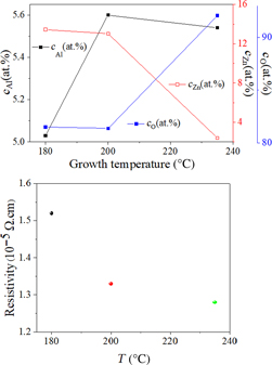
Aluminum-doped zinc oxide films were prepared by atomic layer deposition using diethylzinc, trimethylaluminum, and water. High-purity water was used with low vacuum. The effect of growth temperature on characteristics of the films was investigated. The crystallinity was improved as growth temperature was increased from 180 to 235 °C, with the grain sizes increasing from 32.830 to 47.020 nm. The films possessed high transparency with a 95% transmission window blue shifted with growth temperature. This shift was seen in the energy-band gaps which changed from 3.46 to 3.68 eV, leading to a decreased resistivity from 1.52 × 10⁻⁵ to 1.28 × 10⁻⁵ Ω cm.
Information
- Type
- Research Letters
- Information
- Copyright
- Copyright © Materials Research Society 2019
References
1.Jang, J., Kim, J., Ghorpade, U., Shin, H., Gang, M., Park, S., Kim, H., Lee, D., and Kim, J.: Comparison study of ZnO-based quaternary TCO materials for photovoltaic application. J. Alloys Compd 793, 499–504 (2019). https://doi.org/10.1016/j.jallcom.2019.04.042.Google Scholar
2.Chen, Z., Liu, Y., Zhang, W., Guo, X., Yin, L., Wang, Y., Li, L., Zhang, Y., Wang, Z., and Zhang, T.: Growth of graphene/Ag nanowire/graphene sandwich films for transparent touch-sensitive electrodes. Mater. Chem. Phys. 221, 78 (2019).Google Scholar
3.Ko, D., Gu, B., Cheon, J., Roh, J., Kim, C., Jod, S., Hyun, D., and Kim, J.: Decoupling the contributions to the enhancement of electrical conductivity in transparent silver nanowire/zinc oxide composite electrodes. Mater. Chem. Phys. 223, 634 (2019).Google Scholar
4.Olson, D., Rost, C., Gaskins, J., Szwejkowski, C., Braun, J., and Hopkins, P.: Size effects on the cross-plane thermal conductivity of transparent conducting indium tin oxide and fluorine tin oxide thin films. IEEE Trans. Comp. Pack. Manuf.Technol. 9(1), 51 (2019).Google Scholar
5.Jin, M., Choi, J., Kim, D., Park, J., An, C., Kim, H., Kim, B., Diao, Y., and Jung, H.: Enhanced thermal stability of organic solar cells on nano structured electrode by simple acid etching. Org. Electron. 15, 680 (2014).Google Scholar
6.Solís-Cortés, D., Navarrete-Astorga, E., Costa-Krämer, J.L., Salguero-Fernandez, J., Schrebler, R., Leinen, D., Dalchiele, E.A., Ramos-Barrado, J.R., and Martín, F.: Ga-doped IZO films obtained by magnetron sputtering as transparent conductors for visible and solar applications. Ceram. Int. 45, 5577 (2019).Google Scholar
7.Carlé, J., Helgesen, M., Madsen, M., Bundgaard, E., and Krebs, F.: Upscaling from single cells to modules – fabrication of vacuum- and ITO-free polymer solar cells on flexible substrates with long lifetime. J. Mater. Chem. C 2, 1290 (2014).Google Scholar
8.Khan, F., Baek, S., Mobin, A., and Kim, J.: Enhanced performance of silicon solar cells by application of low-cost sol–gel-derived Al-rich ZnO film. Sol. Energy 101, 265 (2014).Google Scholar
9.Kumarakurua, H., Cherns, D., and Collins, A.: The growth and conductivity of nanostructured ZnO films grown on Al-doped ZnO precursor layers by pulsed laser deposition. Ceram. Int. 40, 8389 (2014).Google Scholar
10.Kumar, K., Ganesh, V., Shkir, M., AlFaify, S., and Valanarasu, S.: Effect of different solvents on the key structural, optical and electronic properties of sol–gel dip coated AZO nanostructured thin films for optoelectronic applications. J. Mater. Sci.: Mater. Electron. 29, 887 (2018).Google Scholar
11.Jilani, A., Abdel-wahab, M.S., Al-ghamdi, A.A., Dahlan, A., and Yahia, I.S.: Nonlinear optical parameters of nanocrystalline AZO thin film measured at different substrate temperatures. Physica B 481, 97 (2016).Google Scholar
12.Choi, Y., Gong, S., Johnson, D., Golledge, S., Yeom, G., and Park, H.: Characteristics of the electromagnetic interference shielding effectiveness of Al-doped ZnO thin films deposited by atomic layer deposition. Appl. Surf. Sci. 269, 92 (2013).Google Scholar
14.Chang, J.F. and Hon, M.H.: The effect of deposition temperature on the properties of Al-doped zinc oxide thin films. Thin Solid Films 386, 79 (2001).Google Scholar
15.Ahn, C., Lee, S., and Cho, H.: Influence of growth temperature on the electrical and structural characteristics of conductive Al-doped ZnO thin films grown by atomic layer deposition. Thin Solid Films 545, 106 (2013).Google Scholar
16.Prabua, R., Valanarasua, S., Ganesh, V., Shkir, M., AlFaify, S., Kathalingam, A., Srikumare, S., and Chandramohan, R.: An effect of temperature on structural, optical, photoluminescence and electrical properties of copper oxide thin films deposited by nebulizer spray pyrolysis technique. Mater. Sci. Semicond. Process. 74, 129 (2018).Google Scholar
17.Barret, C. and Massalki, T.B.: Structure of Metals: Crystallographic Methods, Principles and Data (Pergamon Press, Oxford, UK,1980), p. 204.Google Scholar
18.Dasgupta, N., Neubert, S., Lee, W., Trejo, O., Lee, J., and Prinz, F.: Atomic layer deposition of Al-doped ZnO films: effect of grain orientation on conductivity. Chem. Mater. 22, 4769 (2010).Google Scholar
19.Warren, B.E.: X-Ray Diffraction (Addison-Wesley Publishing Co., London, 1969). p. 18.Google Scholar
20.Barhoumi, A., Leroy, G., Duponchel, B., Gest, J., Yang, L., Waldhoff, N., and Guermazi, S.: Aluminum doped ZnO thin films deposited by direct current sputtering: structural and optical properties. Superlattice. Microstruct. 82, 483 (2015).Google Scholar
21.Steglich, M., Bingel, A., Jia, G., and Falk, F.: Atomic layer deposited ZnO:Al for nanostructured silicon heterojunction solar cells. Sol. Energ. Mater. Sol. Cells 103, 62 (2012).Google Scholar
22.Szyszka, B.: Transparent and conductive aluminum doped zinc oxide films prepared by mid-frequency reactive magnetron sputtering. Thin Solid Films 351, 164 (1999).Google Scholar
23.Balaprakash, V., Gowrisankar, P., Sudha, S., and Rajkumar, R.: Aluminum doped ZnO transparent conducting thin films prepared by sol-gel dip coating technique for solar cells and optoelectronic applications. Mater. Technol. 33, 414 (2018).Google Scholar
24.Gu, T., Hu, E., Guo, S., Wu, Y., Wang, J., Wang, Z., Yua, K., Wei, W., Zheng, Y., Wang, S., and Chen, L.: Ellipsometric study on optical properties of hydrogen plasma-treated aluminum-doped ZnO thin film. Vacuum 163, 69 (2019).Google Scholar
25.Wen, L., Sahu, B., Kim, H., and Han, J.: Study on the electrical, optical, structural, and morphological properties of highly transparent and conductive AZO thin films prepared near room temperature. Appl. Surf. Sci. 473, 649 (2019).Google Scholar
26.Agura, H., Suzuki, A., Matsushita, T., Aoki, T., and Okuda, M.: Low resistivity transparent conducting Al-doped ZnO films prepared by pulsed laser deposition. Thin Solid Films 445, 263 (2003).Google Scholar
27.Kim, H., Osofsky, M., Prokes, S.M., Glembocki, O.J., and Pique, A.: Optimization of Al-doped ZnO films for low loss plasmonic materials at telecommunication wavelengths. Appl. Phys. Lett. 102, 171103 (2013).Google Scholar
28.Vorobyeva, N.A., Rumyantseva, M.N., Vasiliev, R.B., Kozlovskiy, V.F., Soshnikova, Y.M., Filatova, D.G., Zaytsev, V.B., Zaytseva, A.V., and Gaskov, A.M.: Doping effects on electrical and optical properties of spin-coated ZnO thin films. Vacuum 114, 198 (2015).Google Scholar
29.Frank, G. and Kostlin, H.: Electrical-properties and defect model of tin-doped indium oxide layers. Appl. Phys. Mater. Sci. Process. 27(4), 197 (1982).Google Scholar
30.Tauc, J., Grigorovici, R., and Vancu, A.: Optical properties and electronic structure of amorphous germanium. Phys. Status Solidi A 15, 627 (1966).Google Scholar
31.Kim, Y. and Tai, W.: Electrical and optical properties of Al-doped ZnO thin films by sol–gel process. Appl. Surf. Sci. 253, 4911 (2007).Google Scholar
32.Xia, Y., Wang, P., Shi, S., Zhang, M., Hea, G., Lv, J., and Suna, Z.: Deposition and characterization of AZO thin films on flexible glass substrates using DC magnetron sputtering technique. Ceram. Int. 43(5), 4536 (2017).Google Scholar
33.Benramdane, N., Murad, W.A., Misho, R.H., Ziane, M., and Kebbab, Z.: A chemical method for the preparation of thin films of CdO and ZnO. Mater. Chem. Phys. 48, 119–23 (1997).Google Scholar
34.Zheng, H., Zhang, R., Li, D., Chen, X., Wang, S., Zheng, Y., Li, M., Hu, Z., Dai, N., and Chen, L.: Optical properties of Al-doped ZnO films in the infrared region and their absorption applications. Nanoscale Res. Lett. 13, 149 (2018).Google Scholar
35.Mihaiu, S., Toader, A., Anastasescu, M., Gabor, M., Petrisor, T., Stoica, M., and Zaharescu, M.: Al-doped and undoped zinc oxide films obtained by soft chemistry. Process. Appl. Ceram. 3(1-2), 79 (2009).Google Scholar
36.Hodgson, J.: Optical Absorption and Dispersion in Solids (Chapman and Hall Ltd, London, 1970), p. 9.Google Scholar
- 7
- Cited by

