Hostname: page-component-745bb68f8f-5r2nc Total loading time: 0 Render date: 2025-01-14T11:50:52.625Z Has data issue: false hasContentIssue false

200 mm wafer-scale fabrication of polydimethylsiloxane fluidic devices for fluorescence imaging of single DNA molecules

Published online by Cambridge University Press:  11 April 2018

Sung-Wook Nam*
Affiliation:
Department of Molecular Medicine, School of Medicine, Kyungpook National University, Daegu 41405, South Korea
*
Address all correspondence to S.-W. Nam at nams@knu.ac.kr
Get access

Abstract

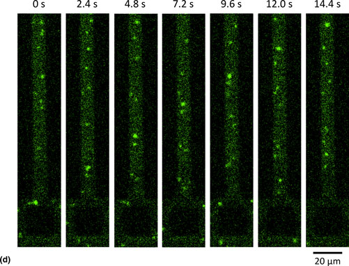
We report fabrication of 200 mm silicon (Si)-wafer mold structure for polydimethylsiloxane (PDMS) microfluidic devices to demonstrate a real-time fluorescence imaging of single DNA molecules. Conventional photolithography with deep reactive ion etching process allows us to build a “mesa”-type Si mold with a nanoscallop sidewall geometry aiding PDMS residue-free process. By optimizing fluorescence microscopy with the fabricated PDMS chamber, we obtain a protocol to visualize the motions of single DNA molecules. This integrative PDMS-based single-molecule imaging system can, in principle, be used as a platform to study biochemical reactions occurring in proteins, nucleotides, and vesicles.

Type
Research Letters
Copyright
Copyright © Materials Research Society 2018 

Access options

Get access to the full version of this content by using one of the access options below. (Log in options will check for institutional or personal access. Content may require purchase if you do not have access.)

References

1.Odom, T.W., Love, J.C., Wolfe, D.B., Paul, K.E., and Whitesides, G.M.: improved pattern transfer in soft lithography using composite stamps. Langmuir 18, 53145320 (2002).Google Scholar
2.Jo, B.-H., Lerberghe, L.M.V., Motsegood, K.M., and Beebe, D.J.: Three-dimensional micro-channel fabrication in polydimethylsiloxane (PDMS) elastomer. J. Micromech. Syst. 9, 7681 (1999).CrossRefGoogle Scholar
3.Chen, X., and Zhang, L.: Review in manufacturing methods of nanochannels of bio-nanofluidic chips. Sens. Actuators B: Chem. 254, 648659 (2018).Google Scholar
4.Dahiya, R., Gottardi, G., and Laidani, N.: PDMS residues-free micro/macrostructures on flexible substrates. Microelectron. Eng. 136, 5762 (2015).CrossRefGoogle Scholar
5.Huh, D., Mills, K.L., Zhu, X., Burns, M.A., Thouless, M.D., and Takayama, S.: Tuneable elastomeric nanochannels for nanofluidic manipulation. Nat. Mater. 6, 424428 (2007).Google Scholar
6.Yang, A.H.J., Moore, S.D., Schmidt, B.S., Klug, M., Lipson, M., and Erickson, E.: Optical manipulation of nanoparticles and biomolecules in sub-wavelength slot waveguides. Nature 457, 7175 (2009).Google Scholar
7.Jo, K., Dhingra, D.M., Odijk, T., de Pablo, J.J., Graham, M.D., Runnheim, R., Forrest, D., and Schwartz, D.C.: A single-molecule barcoding system using nanoslits for DNA analysis. Proc. Natl. Acad. Sci. USA 104, 26732678 (2007).Google Scholar
8.Pedron, S., Polishetty, H., Pritchard, A.M., Mahadik, B.P., Sarkaria, J.N., and Harley, B.A.C.: Spatially graded hydrogels for preclinical testing of glioblastoma anticancer therapeutics. MRS Commun. 7, 442449 (2017).Google Scholar
9.Kang, C.K., Lee, S.M., Jung, I.D., Jung, P.G., Hwang, S.J., and Ko, J.S.: The fabrication of patternable silicon nanotips using deep reactive ion etching. J. Micromech. Microeng. 18, 075007 (2008).CrossRefGoogle Scholar
10.Chen, K.-S., Ayon, A.A., Zhang, X., and Spearing, S.M.: Effect of process parameters on the surface morphology and mechanical performance of silicon structures after deep reactive ion etching (DRIE). J. Microelectromech. Syst. 11, 264275 (2002).CrossRefGoogle Scholar
11.Kim, P., Zarzar, L.D., He, X., Grinthal, A., and Aizenberg, J.: Hydrogel-actuated integrated responsive systems (HAIRS): moving towards adaptive materials. Curr. Opin. Solid State Mater. Sci. 15, 236245 (2011).Google Scholar
12.Wang, C., Nam, S.-W., Cotte, J.M., Jahnes, C.V., Colgan, E.G., Bruce, R.L., Brink, M., Lofaro, M.F., Patel, J.V., Gignac, L.M., Joseph, E.A., Rao, S.P., Stolovitzky, G., Polonsky, S., and Lin, Q.: Wafer-scale integration of sacrificial nanofluidic chips for detecting and manipulating single DNA molecules. Nat. Commun. 8, 14243 (2017).Google Scholar
13.Levy, S.L., Mannion, J.T., Cheng, J., Reccius, C.H., and Craighead, H.G.: Entropic unfolding of DNA molecules in nanofluidic channels. Nano Lett. 8, 38393844 (2008).Google Scholar
14.Kundukad, B., Yan, J., and Doyle, P.S.: Effect of YOYO-1 on the mechanical properties of DNA. Soft Mater. 10, 97219728 (2014).Google Scholar
15.Stein, D., Kruithof, M., and Dekker, C.: Surface-charge-governed ion transport in nanofluidic channels. Phys. Rev. Lett. 93, 035901 (2004).Google Scholar
16.Schoch, R.B. and Renaud, P.: Ion transport through nanoslits dominated by the effective surface charge. Appl. Phys. Lett. 86, 253111 (2005).Google Scholar
17.Nam, S.-W., Rook, M.J., Kim, K.-B., and Rossnagel, S.M.: Ionic field effect transistors with sub-10 nm multiple nanopores. Nano Lett. 9, 20442048 (2009).Google Scholar
18.Nam, S.-W., Lee, M.-H., Lee, S.-H., Lee, D.-J., Rossnagel, S.M., and Kim, K.-B.: Sub-10 nm nanochannels by self-sealing and self-limiting atomic layer deposition. Nano Lett. 10, 33243329 (2010).Google Scholar
19.Schrott, W., Slouka, Z., Cervenka, P., Ston, J., Nebyla, M., Pribyl, M., and Snita, D.: Study on surface properties of PDMS microfluidic chips treated with albumin. Biomicrofluidics 3, 044101 (2009).Google Scholar
20.Wong, I. and Ho, C.-M.: Surface molecular property modifications for poly(dimethylsiloxane) (PDMS) based microfluidic devices. Microfluid. Nanofluid. 7, 291306 (2009).Google Scholar
21.Cao, H., Tegenfeldt, J.O., Austin, R.H., and Chou, S.Y.: Gradient nanostructures for interfacing microfluidics and nanofluidics. Appl. Phys. Lett. 81, 30583060 (2002).CrossRefGoogle Scholar
22.Lam, E.T., Hastie, A., Lin, C., Ehrlich, D., Das, S.K., Austin, M.D., Deshpande, P., Cao, H., Nagarajan, N., Xiao, M., and Kwok, P.-Y.: Genome mapping on nanochannel arrays for structural variation analysis and sequence assembly. Nat. Biotechnol. 30, 771776 (2012).Google Scholar
23.Jeffet, J., Kobo, A., Su, T., Grunwald, A., Green, O., Nilsson, A.N., Eisenberg, E., Ambjornsson, T., Westerlund, F., Weinhold, E., Shabat, D., Purohit, P.K., and Ebenstein, Y.: Super-resolution genome mapping in silicon nanochannels. ACS Nano 10, 98239830 (2016).Google Scholar
24.Bakajin, O.B., Duke, T.A.J., Chou, C.F., Chan, S.S., Austin, R.H., and Cox, E.C.: Electrohydrodynamic stretching of DNA in confined environments. Phys. Rev. Lett. 80, 27372740 (1998).Google Scholar
25.Houseal, T.W., Bustamante, C., Stump, R.F., and Maestre, M.F.: Real-time imaging of single DNA molecules with fluorescence microscopy. Biophys. J. 56, 507516 (1989).Google Scholar
26.Macosko, E.Z., Basu, A., Satija, R., Nemesh, J., Shekhar, K., Goldman, M., Tirosh, I., Bialas, A.R., Kamitaki, N., Martersteck, E.M., Trombetta, J.J., Weitz, D.A., Sanes, J.R., Shalek, A.K., Regev, A., and McCarroll, S.A.: Highly parallel genome-wide expression profiling of individual cells using nanoliter droplets. Cell 161, 12021214 (2015).Google Scholar
27.Yelleswarapu, V.R., Jeong, H.-H., Yadavali, S., and Issadore, D.: Ultra-high throughput detection (1 million droplets per second) of fluorescent droplets using a cell phone camera and time domain encoded optofluidics. Lab Chip 17, 10831094 (2017).Google Scholar
28.Frankowski, M., Simon, P., Bock, N., El-hasni, A., Schnakenberg, U., and Neukammer, J.: Simultaneous optical and impedance analysis of single cells: a comparison of two microfluidic sensors with sheath flow focusing. Eng. Life Sci. 15, 286296 (2015).Google Scholar
29.Wi, J.-S., Park, J., Kang, H., Jung, D., Lee, S.-W., and Lee, T.G.: Stacked gold nanodisks for bimodal photoacoustic and optical coherence imaging. ACS Nano 11, 62256232 (2017).Google Scholar
30.Keyser, U.F., Koeleman, B.N., Dorp, S.V., Krapf, D., Smeets, R.M.M., Lemay, S.G., Dekker, N.H., and Dekker, C.: Direct force measurements on DNA in a solid-state nanopore. Nat. Phys. 2, 473477 (2006).Google Scholar
31.Bai, J., Wang, D., Nam, S., Peng, H., Bruce, R., Gignac, L., Brink, M., Kratschmer, E., Rossnagel, S., Waggoner, P., Reuter, K., Wang, C., Astier, Y., Balagurusamy, V., Luan, B., Kwark, Y., Joseph, E., Guillorn, M., Polonsky, S., Royyuru, A., Rao, S.P., and Stolovitzky, G.: Fabrication of sub-20 nm nanopore array in membranes with embedded metal electrodes at wafer scales. Nanoscale 6, 89008906 (2014).CrossRefGoogle ScholarPubMed
32.Schermelleh, L., Heintzmann, R., and Leonhardt, H.: A guide to super-resolution fluorescence microscopy. J. Cell Biol. 190, 165175 (2010).Google Scholar
33.Chen, J., Xu, Y., Lv, X., Lai, X., and Zeng, S.: Super-resolution differential interference contrast microscopy by structured illumination. Opt. Express 21, 112121 (2013).Google Scholar
34.Wang, G., Sun, W., Luo, Y., and Fang, N.: Resolving rotational motions of nano-objects in engineered environments and live cells with gold nanorods and differential interference contrast microscopy. J. Am. Chem. Soc. 132, 1641716422 (2010).Google Scholar
Supplementary material: PDF

Nam supplementary material

Supplementary Information

Download Nam supplementary material(PDF)
PDF 665.2 KB

Nam supplementary material

Movie S1

Download Nam supplementary material(Video)
Video 4.4 MB

Nam supplementary material

Movie S2

Download Nam supplementary material(Video)
Video 8.7 MB