Hostname: page-component-745bb68f8f-5r2nc Total loading time: 0 Render date: 2025-01-12T05:25:14.817Z Has data issue: false hasContentIssue false

Nucleation and growth of metamorphic epitaxial aluminum on silicon (111) 7 × 7 and $\sqrt 3 \times \sqrt 3$ surfaces

Published online by Cambridge University Press:  21 August 2017
Ashish Alexander*
Affiliation:
Laboratory for Physical Sciences, University of Maryland, College Park, Maryland 20740, USA
Brian M. McSkimming
Affiliation:
Laboratory for Physical Sciences, University of Maryland, College Park, Maryland 20740, USA
Bruce Arey
Affiliation:
Pacific Northwest National Laboratory, Richland, Washington 99352, USA
Ilke Arslan
Affiliation:
Pacific Northwest National Laboratory, Richland, Washington 99352, USA
Christopher J.K. Richardson
Affiliation:
Laboratory for Physical Sciences, University of Maryland, College Park, Maryland 20740, USA
*
a)Address all correspondence to this author. e-mail: aalex@lps.umd.edu
Get access

Abstract

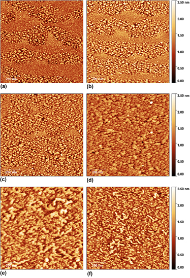
The nucleation and growth of Al on 7 × 7 and $\sqrt 3 \times \sqrt 3$R30 Al reconstructed Si(111) that result in strain-free Al overgrown films grown with an atomically abrupt metamorphic interface are compared. The reconstructed surfaces and abrupt strain relaxations are verified using reflection high-energy electron diffraction. The topography of evolution is examined with atomic force microscopy. The growth of Al on both the surfaces exhibits 3D island growth, but the island evolution of growth is dramatically different. On the 7 × 7 surface, mounds formed are uniformly distributed across the substrate, and growth appears to proceed uniformly. Alternatively, on the $\sqrt 3 \times \sqrt 3$R30 surface, Al atoms exhibit a clear preference to form mounds near the step edges. During Al growth, mounds increase in size and number, expanding out from step edges until they cover the whole substrate. Consistent expression of a mounded nucleation and growth mode imparts a physical limitation to the achievable surface roughness that may impact the ultimate performance of layered devices such as Josephson junctions that are critical components of superconducting quantum circuits.

Type
Invited Articles
Copyright
Copyright © Materials Research Society 2017 

Access options

Get access to the full version of this content by using one of the access options below. (Log in options will check for institutional or personal access. Content may require purchase if you do not have access.)

Footnotes

Contributing Editor: Artur Braun

References

REFERENCES

Richardson, C.J.K. and Lee, M.L.: Metamorphic epitaxial materials. MRS Bull. 41, 193 (2016).CrossRefGoogle Scholar
Frank, F.C. and van der Merwe, J.H.: One-dimensional dislocations. I. Static theory. Proc. R. Soc. London, Ser. A 198, 205 (1949).Google Scholar
Frank, F.C. and van der Merwe, J.H.: One-dimensional dislocations. II. Misfitting monolayers and oriented overgrowth. Proc. R. Soc. London, Ser. A 198, 216 (1949).Google Scholar
Woltersdorf, J.: Misfit accommodation at interfaces by dislocations. Appl. Surf. Sci. 11/12, 495 (1982).Google Scholar
Johnson, G.R., Cavenett, B.C., Kerr, T.M., Kirby, P.B., and Wood, C.E.C.: Optical, Hall and cyclotron resonance measurements of GaSb grown by molecular beam epitaxy. Semicond. Sci. Technol. 3, 1157 (1988).Google Scholar
Ivanov, S.V., Altukhov, P.D., Argunova, T.S., Bakun, A.A., Budza, A.A., Chaldyshev, V.V., Kovalenko, Y.A., Kop’ev, P.S., Kutt, R.N., Meltser, B.Y., Ruvimov, S.S., Shaposhnikov, S.V., Sorokin, L.M., and Ustinov, V.M.: Molecular beam epitaxy growth and characterization of thin (<2 µm) GaSb 1 layers on GaAs(100) substrates. Semicond. Sci. Technol. 8, 347 (1993).Google Scholar
Trampert, A., Tounrié, E., and Ploog, K.H.: Novel plastic strain-relaxation mode in highly mismatched III–V layers induced by two-dimensional epitaxial growth. Appl. Phys. Lett. 66(17), 2265 (1995).CrossRefGoogle Scholar
Richardson, C.J.K., He, L., and Kanakraju, S.: Metamorphic growth of III–V semiconductor bicrystals. J. Vac. Sci. Technol., B: Nanotechnol. Microelectron.: Mater., Process., Meas., Phenom. 29(3), 03C126 (2011).Google Scholar
Mehta, M., Balakrishnan, G., Huang, S., Khoshakhlagh, A., Jallipalli, A., Patel, P., Kutty, M.N., Dawson, L.R., and Huffaker, D.L.: GaSb quantum-well-based “buffer-free” vertical light emitting diode monolithically embedded within a GaAs cavity incorporating interfacial misfit arrays. Appl. Phys. Lett. 89, 211110 (2006).Google Scholar
Richardson, C.J.K., He, L., Apiratikul, P., Siwak, N.P., and Leavitt, R.P.: Improved GaSb-based quantum well laser performance through metamorphic growth on GaAs substrates. Appl. Phys. Lett. 106, 101108 (2015).Google Scholar
Edirisooriya, M., Mishima, T.D., Gaspe, C.K., Bottoms, K., Hauenstein, R.J., and Santos, M.B.: InSb quantum-well structures for electronic device applications. J. Cryst. Growth 311, 1972 (2009).CrossRefGoogle Scholar
van der Merwe, J.H.: Crystal interfaces. Part I. Semi-infinite crystals. J. Appl. Phys. 34(1), 117 (1963).Google Scholar
van der Merwe, J.H.: Crystal interfaces. Part II. Finite overgrowths. J. Appl. Phys. 34(1), 123 (1963).Google Scholar
Jesser, W.A. and van der Merwe, J.H.: The size dependence of equilibrium elastic strain in finite epitaxial islands. Surf. Sci. 31, 229 (1972).Google Scholar
Snyman, J.A. and Snyman, H.C.: Computed epitaxial monolayer structures III. Two-dimensional model: Zero average strain monolayer structures in the case of hexagonal interfacial symmetry. Surf. Sci. 105, 357 (1981).CrossRefGoogle Scholar
van der Merwe, J.H.: Theoretical considerations in growing uniform epilayers. Interface Sci. 1, 77 (1993).Google Scholar
Danescu, A., Gobaut, B., Penuelas, J., Grenet, G., Favre-Nicolin, V., Blanc, N., Zhou, T., Renaud, G., and Saint-Girons, G.: Interface accommodation mechanism for weakly interacting epitaxial systems. Appl. Phys. Lett. 103, 021602 (2013).CrossRefGoogle Scholar
Pilania, G., Thijsse, B.J., Hoagland, R.G., Lazic, I., Valone, S., and Liu, X-Y.: Revisiting the Al/Al2O3 Interface: Coherent interfaces and misfit accommodation. Sci. Rep. 4, 4485 (2014).CrossRefGoogle ScholarPubMed
Koch, J., Yu, T.M., Gambetta, J., Houck, A.A., Schuster, D.I., Majer, J., Blais, A., Devoret, M.H., Girvin, S.M., and Schoelkopf, R.J.: Charge-insensitive qubit design derived from the Cooper pair box. Phys. Rev. A 76, 042319 (2007).Google Scholar
Barends, R., Kelly, J., Megrant, A., Veitia, A., Sank, D., Jeffrey, E., White, T.C., Mutus, J., Fowler, A.G., Campbell, B., Chen, Y., Chen, Z., Chiaro, B., Dunsworth, A., Neill, C., O’Malley, P., Roushan, P., Vainsencher, A., Wenner, J., Korotkov, A.N., Cleland, A.N., and Martinis, J.M.: Superconducting quantum circuits at the surface code threshold for fault tolerance. Nature 508, 500 (2014).CrossRefGoogle ScholarPubMed
Blais, A., Huan, R-S., Wallraff, A., Givin, S.M., and Schoelkopf, R.J.: Cavity quantum electrodynamics for superconducting electrical circuits: An architecture for quantum computation. Phys. Rev. A 69, 062320 (2004).CrossRefGoogle Scholar
Megrant, A., Neill, C., Barends, R., Chiaro, B., Chen, Y., Feigl, L., Kelly, J., Lucero, E., Mariantoni, M., O’Malley, P.J.J., Sank, D., Vainsencher, A., Wenner, J., White, T.C., Yin, Y., Zhao, J., Palmstrøm, C.J., Martinis, J.M., and Cleland, A.N.: Planar superconducting resonators with internal quality factors above one million. Appl. Phys. Lett. 100, 113510 (2012).Google Scholar
Quintana, C.M., Megrant, A., Chen, Z., Dunsworth, A., Chiaro, B., Barends, R., Campbell, B., Chen, Y., Hoi, I-C., Jeffrey, E., Kelly, J., Mutus, J.Y., O’Malley, P.J.J., Neill, C., Roushan, P., Sank, D., Vainsencher, A., Wenner, J., White, T.C., Cleland, A.N., and Martinis, J.M.: Characterization and reduction of microfabrication-induced decoherence in superconducting quantum circuits. Appl. Phys. Lett. 105, 062601 (2014).Google Scholar
Richardson, C.J.K., Siwak, N.P., Hackley, J., Keane, Z.K., Robinson, J.E., Arey, B., Arslan, I., and Palmer, B.S.: Fabrication artifacts and parallel loss channels in metamorphic epitaxial aluminum superconducting resonators. Supercond. Sci. Technol. 29, 064003 (2016).CrossRefGoogle Scholar
Gao, J., Daal, M., Vayonakis, A., Kumar, S., Zmuidzinas, J., Sadoulet, B., Mazin, B.A., Day, P.K., and Leduc, H.G.: Experimental evidence for a surface distribution of two-level systems in superconducting lithographed microwave resonators. Appl. Phys. Lett. 92, 152505 (2008).CrossRefGoogle Scholar
Wenner, J., Barends, R., Bialczak, R.C., Chen, Y., Kelly, J., Lucero, E., Mariantoni, M., Megrant, A., O’Malley, P.J.J., Sank, D., Vainsencher, A., Wang, H., White, T.C., Tin, Y., Zhao, J., Cleland, A.N., and Martinis, J.M.: Surface loss simulations of superconducting coplanar waveguide resonators. Appl. Phys. Lett. 99, 113513 (2011).CrossRefGoogle Scholar
Zeng, L.J., Nik, S., Greibe, T., Krantz, P., Wilson, C.M., Delsing, P., and Olsson, E.: Direct observation of the thickness distribution of ultra-thin AlO x barriers in Al/AlO x /Al Josephson junctions. J. Phys. D: Appl. Phys. 48, 395308 (2015).Google Scholar
Horio, Y.: Structural study of Al deposited surface in Si(111) $\sqrt 3 \times \sqrt 3$ –Al. Appl. Surf. Sci. 169–170, 104 (2001).Google Scholar
Horio, Y.: Different growth modes of Al on Si(111) 7 × 7 and Si(111) $\sqrt 3 \times \sqrt 3$ –Al surfaces. Jpn. J. Appl. Phys., Part 1 38(8), 4881 (1999).Google Scholar
Horio, Y.: Surface morphology of growing Al on Si(111) 7 × 7 and Si(111) $\sqrt 3 \times \sqrt 3$ –Al substrates by reflection high-energy electron diffraction. Jpn. J. Appl. Phys., Part 1 39(7B), 4374 (2000).Google Scholar
Lander, J.J. and Morrison, J.: Surface reactions of silicon with aluminum and with indium. Surf. Sci. 2, 553 (1964).Google Scholar
McSkimming, B.M., Alexander, A., Samuels, M.H., Arey, B., Arslan, I., and Richardson, C.J.K.: Metamorphic growth of relaxed single crystalline aluminum on silicon (111). J. Vac. Sci. Technol., A 35(2), 021401 (2017).Google Scholar
Higashi, G.S., Becker, R.S., Chabal, Y.J., and Becker, A.J.: Comparison of Si(111) surfaces prepared using aqueous solutions of NH4F versus HF. Appl. Phys. Lett. 58(15), 1656 (1991).CrossRefGoogle Scholar
Ali, D. and Richardson, C.J.K.: Reflection high-energy electron diffraction evaluation of thermal deoxidation of chemically cleaned Si, SiGe, and Ge layers for solid-source molecular beam epitaxy. J. Vac. Sci. Technol., A 30(6), 061405 (2012).Google Scholar
Mizutani, T.: Correct substrate temperature monitoring with infrared optical pyrometer for molecular-beam epitaxy of III–V semiconductors. J. Vac. Sci. Technol., B: Microelectron. Process. Phenom. 6(6), 1671 (1988).Google Scholar
Ohring, M.: The Material Science of Thin Films Deposition and Structure, 2nd ed. (Academic Press, San Diego, California, 2002); p. 378.Google Scholar
van der Merwe, J.H.: Equilibrium structure of a thin epitaxial film. J. Appl. Phys. 41(11), 4725 (1970).Google Scholar
Haynes, W.M., ed.: Enthalpy of fusion. In CRC Handbook of Chemistry and Physics, 97th ed. (CRC Press/Taylor & Francis, Boca Raton, Florida, 2017).Google Scholar
Tang, F.L., Cheng, X.G., Lu, W.J., and Yu, W.Y.: Premelting of Al nonperfect (111) surface. Phys. B 405, 1248 (2010).Google Scholar
Takayanagi, K., Tanishiro, Y., Takahashi, S., and Takahashi, M.: Structure analysis of Si(111)-7 × 7 reconstructed surface by transmission electron diffraction. Surf. Sci. 164, 367 (1985).Google Scholar
Uemura, A., Ohkita, A., Inaba, H., Hasegawa, S., and Nakashima, H.: Effects of Si reconstruction on growth mode in A1/Si(111) studied by scanning tunneling microscopy. Surf. Sci. 357–358, 825 (1996).Google Scholar
Wang, S., Radny, M.W., and Smith, P.V.: Mechanisms for the stability of Al and B adatoms on the Si(111) $\sqrt 3 \times \sqrt 3 \;R{30^\circ }$ surface. Phys. Rev. B 59(3), 1594 (1999).Google Scholar
Northrup, J.E.: Si(111) $\sqrt 3 \times \sqrt 3$ –Al: An adatom-induced reconstruction. Phys. Rev. Lett. 53(7), 683 (1984).Google Scholar
Hanada, T., Daimon, H., and Ino, S.: Rocking-curve analysis of reflection high-energy electron diffraction from the Si(111)– $\left( {\sqrt 3 \times \sqrt 3 } \right)R{30^\circ }$ –Al, –Ga and –In surfaces. Phys. Rev. B 51(19), 13320 (1995).CrossRefGoogle Scholar
Hoshino, T., Okano, K., Enomoto, N., Hata, M., and Tsuda, M.: Migration process of an Al adatom on the Si(111) surface. Surf. Sci. 423, 117 (1999).Google Scholar