Hostname: page-component-745bb68f8f-d8cs5 Total loading time: 0 Render date: 2025-01-26T23:26:43.479Z Has data issue: false hasContentIssue false

Emission of partial dislocations in silicon under nanoindentation

Published online by Cambridge University Press:  22 July 2013

Qihong Fang
Affiliation:
State Key Laboratory of Advanced Design and Manufacturing for Vehicle Body, Hunan University, Changsha 410082, China
Liangchi Zhang*
Affiliation:
School of Mechanical and Manufacturing Engineering, The University of New South Wales, New South Wales 2052, Australia
*
a)Address all correspondence to this author. e-mail: Liangchi.Zhang@unsw.edu.au
Get access

Abstract

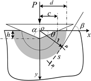
This paper investigates the critical loading condition that causes the emission of dislocations in silicon subjected to nanoindentation. A theoretical model is established, which follows the deformation process that with increasing the indentation load, a phase transformation takes place, followed by partial dislocations emitting from the interface between the phase-transformed zone and the originally crystalline silicon when the indentation load reaches a critical value. In the model, the emission process represents the generation of a dipole of Shockley partial dislocations. One partial dislocation of the dipole, located at the interface, is considered immobile, whereas the other partial dislocation moves into the bulk of silicon. The effects of the indenter geometry and of the location of dislocation nucleation on the critical indentation load are discussed. The model predicts that a sharp indenter leads to a relatively smaller critical indentation load. The model prediction is verified by an indentation experiment.

Type
Articles
Copyright
Copyright © Materials Research Society 2013 

Access options

Get access to the full version of this content by using one of the access options below. (Log in options will check for institutional or personal access. Content may require purchase if you do not have access.)

References

REFERENCES

Petersen, K.E.: Silicon as a mechanical material. Proc. IEEE 70, 420 (1982).CrossRefGoogle Scholar
Blanco, A., Chomski, E., Grabtchak, S., Ibisate, M., John, S., and Leonard, S.W.: Large-scale synthesis of a silicon photonic crystal with a complete three-dimensional bandgap near 1.5 micrometres. Nature 405, 437 (2000).CrossRefGoogle ScholarPubMed
Gerk, A.P. and Tabor, D.: Indentation hardness and semiconductor–metal transition of germanium and silicon. Nature 271, 732 (1978).CrossRefGoogle Scholar
Pharr, G.M., Oliver, W.C., and Clarke, D.R.: The mechanical behavior of silicon during small-scale indentation. J. Electron. Mater. 19, 881 (1990).CrossRefGoogle Scholar
Pharr, G.M., Oliver, W.C., and Harding, D.S.: New evidence for a pressure-induced phase transformation during the indentation of silicon. J. Mater. Res. 6, 1129 (1991).CrossRefGoogle Scholar
Page, T., Oliver, W.C., and McHargue, C.J.: The deformation behavior of ceramic crystals subjected to very low load (nano) indentations. J. Mater. Res. 7, 450 (1992).CrossRefGoogle Scholar
Weppelmann, E.R., Field, J.S., and Swain, M.V.: Influence of spherical indenter radius on the indentation-induced transformation behaviour of silicon. J. Mater. Sci. 30, 2455 (1995).CrossRefGoogle Scholar
Williams, J.S., Chen, Y., Wong-Leung, J., Kerr, A., and Swain, M.V.: Ultra-micro-indentation of silicon and compound semiconductors with spherical indenters. J. Mater. Res. 14, 2338 (1999).CrossRefGoogle Scholar
Li, X.D., Bhushan, B., Takashima, K., Baek, C.W., and Kim, Y.K.: Mechanical characterization of micro/nanoscale structures for MEMS/NEMS applications using nanoindentation techniques. Ultramicroscopy 97, 481 (2003).CrossRefGoogle ScholarPubMed
Fang, T.H., Chang, W.J., and Lin, C.M.: Nanoindentation and nanoscratch characteristics of Si and GaAs. Microelectron. Eng. 77, 389 (2005).CrossRefGoogle Scholar
Zhang, L.C. and Zarudi, I.: Towards a deeper understanding of plastic deformation in mono-crystalline silicon. Int. J. Mech. Sci. 43, 1985 (2001).CrossRefGoogle Scholar
Kailer, A., Gogotsi, Y.G., and Nickel, K.G.: Phase transformations of silicon caused by contact loading. J. Appl. Phys. 87, 3057 (1997).CrossRefGoogle Scholar
Zarudi, I. and Zhang, L.C.: Structure changes in mono-crystalline silicon subjected to indentation -experimental findings. Tribol. Int. 32, 701 (1999).CrossRefGoogle Scholar
Zhang, L.C. and Tanaka, H.: Atomic scale deformation in silicon monocrystals induced by two-body and three-body contact sliding. Tribol. Int. 31, 425433 (1998).CrossRefGoogle Scholar
Zhang, L.C. and Tanaka, H.: On the mechanics and physics in the nano-indentation of silicon mono-crystals. JSME Int J., Ser. A 42, 546559 (1999).CrossRefGoogle Scholar
Juliano, T., Domnich, V., and Gogotsi, Y.: Examining pressure-induced phase transformations in silicon by spherical indentation and Raman spectroscopy: A statistical study. J. Mater. Res. 19, 3099 (2004).CrossRefGoogle Scholar
Jang, J., Lance, M.J., Wen, S., Tsui, T.Y., and Pharr, G.M.: Indentation-induced phase transformations in silicon: Influences of load, rate and indenter angle on the transformation behavior. Acta Mater. 53, 1759 (2005).CrossRefGoogle Scholar
Gerbig, Y.B., Michaels, C.A., Forster, A.M., and Cook, R.F.: In situ observation of the indentation-induced phase transformation of silicon thin films. Phys. Rev. B 85, 104102 (2012).CrossRefGoogle Scholar
Chang, L. and Zhang, L.C.: Mechanical behaviour characterisation of silicon and effect of loading rate on pop-in: A nanoindentation study under ultra-low loads. Mater. Sci. Eng., A 506, 125 (2009).CrossRefGoogle Scholar
Zhang, L.C., Biddut, A.Q., and Ali, Y.M.: Dependence of pad performance on its texture in polishing mono-crystalline silicon wafers. Int. J. Mech. Sci. 52, 657662 (2010).CrossRefGoogle Scholar
Biddut, A., Zhang, L.C., Ali, Y.M., and Liu, Z.: Damage-free polishing of monocrystalline silicon wafers without chemical additives. Scr. Mater. 59, 11781181 (2008).CrossRefGoogle Scholar
Bradby, J.E., Williams, J.S., Wong-Leung, J., Swain, M.V., and Munroe, P.: Transmission electron microscopy observation of deformation microstructure under spherical indentation in silicon. Appl. Phys. Lett. 77, 3749 (2000).CrossRefGoogle Scholar
Bradby, J.E., Williams, J.S., Wong-Leung, J., Swain, M.V., and Munroe, P.: Mechanical deformation in silicon by micro-indentation. J. Mater. Res. 16, 1500 (2001).CrossRefGoogle Scholar
Lloyd, S.J., Molina-Aldareguia, J.M., and Clegg, W.J.: Deformation under nanoindents in Si, Ge, and GaAs examined through transmission electron microscopy. J. Mater. Res. 16, 3347 (2001).CrossRefGoogle Scholar
Lloyd, S.J., Castellero, A., Giuliani, F., Long, Y., McLaughlin, K.K., Molina-Aldareguia, J.M., Stelmashenko, N.A., Vandeperre, L.J., and Clegg, W.J.: Observations of nanoindents via cross-sectionaltransmission electron microscopy: A survey of deformation mechanisms. Proc. R. Soc. London, Ser. A 461, 2521 (2005).Google Scholar
Zarudi, I., Zhang, L.C., Cheong, W.C.D., and Yu, T.X.: The difference of phase distributions in silicon after indentation with Berkovich and spherical indenters. Acta Mater. 53, 4795 (2005).CrossRefGoogle Scholar
Wan, H., Shen, Y., Chen, Q., and Chen, Y.: A plastic damage model for finite element analysis of cracking of silicon under indentation. J. Mater. Res. 25, 2224 (2010).CrossRefGoogle Scholar
Jian, S.R.: Mechanical deformation induced in Si and GaN under Berkovich nanoindentation. Nanoscale Res. Lett. 3, 6 (2008).CrossRefGoogle Scholar
Jang, J. and Pharr, G.M.: Influence of indenter angle on cracking in Si and Ge during nanoindentation. Acta Mater. 56, 4458 (2008).CrossRefGoogle Scholar
Gerberich, W.W., Nelson, J.C., Lilleodden, E.T., Anderson, P., and Wyrobek, J.T.: Indentation induced dislocation nucleation: The initial yield point. Acta Mater. 44, 3585 (1996).CrossRefGoogle Scholar
Tadmor, E.B., Miller, R., Phillips, R., and Ortiz, M.: Nanoindentation and incipient plasticity. J. Mater. Res. 14, 2233 (1999).CrossRefGoogle Scholar
Shenoy, V.B., Phillips, R., and Tadmor, E.B.: Nucleation of dislocations beneath a plane strain indenter. J. Mech. Phys. Solids 48, 649 (2000).CrossRefGoogle Scholar
Zhu, T., Li, J., Vliet, K., Ogata, S., Yip, S., and Suresh, S.: Predictive modeling of nanoindentation-induced homogeneous dislocation nucleation in copper. J. Mech. Phys. Solids 52, 691 (2004).CrossRefGoogle Scholar
Schuh, C.A., Mason, J.K., and Lund, A.C.: Quantitative insight into dislocation nucleation from high temperature nanoindentation experiments. Nature Mater. 4, 617 (2005).CrossRefGoogle ScholarPubMed
Nicola, L., Bower, A.F., Kim, K-S., Needleman, A., and Van der Giessen, E.: Surface versus bulk nucleation of dislocations during contact. J. Mech. Phys. Solids 55, 1120 (2007).CrossRefGoogle Scholar
Begau, C., Hartmaier, A., George, E.P., and Pharr, G.M.: Atomistic processes of dislocation generation and plastic deformation during nanoindentation. Acta Mater. 59, 934 (2011).CrossRefGoogle Scholar
Minor, A.M., Syed Asif, S.A., Shan, Z., Stach, E.A., Cyrankowski, E., Wyrobek, T.J., and Warren, O. L.: A new view of the onset of plasticity during the nanoindentation of aluminium. Nature Mater. 5, 697 (2006).CrossRefGoogle ScholarPubMed
Lorenz, D., Zeckzer, A., Hilpert, U., Grau, P., Johansen, H., and Leipner, H.S.: Pop-in effect as homogeneous nucleation of dislocations during nanoindentation. Phys. Rev. B 67, 172101 (2003).CrossRefGoogle Scholar
Gassilloud, R., Ballif, C., Gasser, P., Buerki, G., and Michler, J.: Deformation mechanisms of silicon during nanoscratching. Phys. Status Solidi A 202, 2858 (2005).CrossRefGoogle Scholar
Wu, Y.Q., Huang, H., Zou, J., and Dell, J.M.: Nanoscratch-induced deformation of single crystal silicon. J. Vac. Sci. Technol., B 27, 1374 (2009).CrossRefGoogle Scholar
Wu, Y.Q., Huang, H., Zou, J., Zhang, L.C., and Dell, J.M.: Nanoscratch-induced phase transformation of monocrystalline Si. Scr. Mater. 63, 847 (2010).CrossRefGoogle Scholar
Wasmer, K., Gassilloud, R., Michler, J., and Ballif, C.: Analysis of onset of dislocation nucleation during nanoindentation and nanoscratching of InP. J. Mater. Res. 27, 320 (2012).CrossRefGoogle Scholar
Minor, A.M., Lilleodden, E.T., Jin, M., Stach, E.A., Chrzan, D.C., and Morris, J.W. Jr.: Room temperature dislocation plasticity in silicon. Philos. Mag. 85, 323 (2005).CrossRefGoogle Scholar
Ge, D., Minor, A.M., Stach, E.A., and Morris, J.W. Jr.: Size effects in the nanoindentation of silicon at ambient temperature. Philos. Mag. 86, 4069 (2006).CrossRefGoogle Scholar
Deneen, J., Mook, W.M., Minor, A., Gerberich, W.W., and Carter, C.B.: In situ deformation of silicon nanospheres. J. Mater. Sci. 41, 4477 (2006).CrossRefGoogle Scholar
Stauffer, D.D., Beaber, A., Wagner, A., Ugurlu, O., Nowak, J., Mkhoyan, K.A., Girshick, S., and Gerberich, W.: Strain-hardening in submicron silicon pillars and spheres. Acta Mater. 60, 2471 (2012).CrossRefGoogle Scholar
Stauffer, D.D.: Deformation mechanisms in nanoscale brittle materials, Ph.D. Thesis, University of Minnesota, Minnesota, 2011.Google Scholar
Gerberich, W.W., Stauffer, D.D., Beaber, A.R., and Tymiak, N.I.: A brittleness transition in silicon due to scale. J. Mater. Res. 27, 552 (2012).CrossRefGoogle Scholar
Garcia-Manyes, S., Güell, A.G., Gorostiza, P., and Sanz, F.: Nanomechanics of silicon surfaces with atomic force microscopy: An insight to the first stages of plastic deformation. J. Chem. Phys. 123, 114711 (2005).CrossRefGoogle Scholar
Ovid’ko, I.A. and Skiba, N.V.: Enhanced dislocation emission from grain boundaries in nanocrystalline materials. Scr. Mater. 67, 13 (2012).CrossRefGoogle Scholar
Bobylev, S.V., Mukherjeeb, A.K., and Ovid’ko, I.A.: Emission of partial dislocations from amorphous intergranular boundaries in deformed nanocrystalline ceramics. Scr. Mater. 60, 36 (2009).CrossRefGoogle Scholar
Hirth, J.P. and Lothe, J.: Theory of Dislocations (McGraw-Hill, New York, 1967).Google Scholar
Freund, L.B. and Suresh, S.: Thin Film Materials: Stress, Defect Formation and Surface Evolution (Cambridge University Press, Cambridge, 2003).Google Scholar
Galanov, B.A., Domnich, V., and Gogotsi, Y.: Elastic-plastic contact mechanics of indentations accounting for phase transformations. Exp. Mech. 43, 303 (2003).Google Scholar
Vdenitcharova, T. and Zhang, L.C.: A new constitutive model for the phase transformations in mono-crystalline silicon. Int. J. Solids Struct. 41, 54115424 (2004).CrossRefGoogle Scholar
Vodenitcharova, T. and Zhang, L.C.: A mechanics prediction of the behaviour of mono-crystalline silicon under nano-indentation. Int. J. Solids Struct. 40, 29892998 (2003).CrossRefGoogle Scholar
Yoffe, E.H.: Elastic stress-fields caused by indenting brittle materials. Philos. Mag. A 46, 617 (1982).CrossRefGoogle Scholar
Feng, G., Qu, S., Huang, Y., and Nix, W.D.: An analytical expression for the stress field around an elastoplastic indentation/contact. Acta Mater. 55, 2929 (2007).CrossRefGoogle Scholar
Feng, G., Qu, S., Huang, Y., and Nix, W.D.: A quantitative analysis for the stress field around an elastoplastic indentation/contact. J. Mater. Res. 24, 704 (2009).CrossRefGoogle Scholar