Skip to main content Accessibility help
×
Hostname: page-component-745bb68f8f-f46jp Total loading time: 0 Render date: 2025-01-11T06:20:51.719Z Has data issue: false hasContentIssue false

10 - Photonic circuitry

from Part II - Advances and challenges

Published online by Cambridge University Press:  23 November 2018

Sergey V. Gaponenko
Affiliation:
National Academy of Sciences of Belarus
Hilmi Volkan Demir
Affiliation:
Nanyang Technological University, Singapore
Get access

Summary

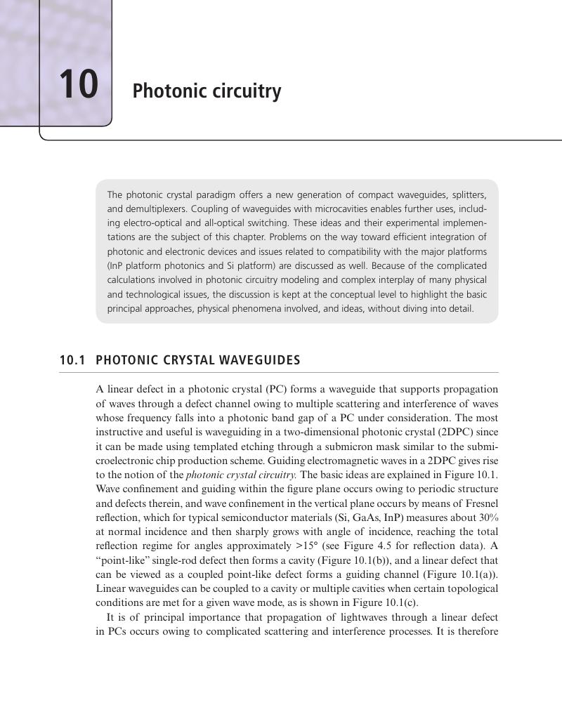
Image of the first page of this content. For PDF version, please use the ‘Save PDF’ preceeding this image.'
Type
Chapter
Information
Applied Nanophotonics , pp. 342 - 362
Publisher: Cambridge University Press
Print publication year: 2018

Access options

Get access to the full version of this content by using one of the access options below. (Log in options will check for institutional or personal access. Content may require purchase if you do not have access.)

References

Further reading

Bozhevolnyi, S. I. (ed.) (2009). Plasmonic Nanoguides and Circuits. Pan Stanford Publishing.Google Scholar
Gilardi, G., and Smit, M. K. (2014). Generic InP-based integration technology: present and prospects. Progr Electromagnetics Res, 147, 2335.Google Scholar
Gramotnev, D. K., and Bozhevolnyi, S. I. (2010). Plasmonics beyond the diffraction limit. Nat Photonics, 4, 8391.CrossRefGoogle Scholar
Jin, C. Y., and Wada, O. (2014). Photonic switching devices based on semiconductor nanostructures. J Physics D: Applied Physics, 47, 133001.CrossRefGoogle Scholar
Krauss, T. F. (2008). Why do we need slow light? Nat Photonics, 2, 448450.CrossRefGoogle Scholar
MacDonald, K. F., and Zheludev, N. I. (2010). Active plasmonics: current status. Laser Photonics Rev, 4, 562567.Google Scholar
Miller, D. A. B. (2009). Device requirements for optical interconnects to silicon chips. Proc IEEE, 97, 11661185.Google Scholar
Mingaleev, S. F., Miroshnichenko, A. E., and Kivshar, Yu. S (2007). Low-threshold bistability of slow light in photonic-crystal waveguides. Opt Express, 15, 1238012385.Google Scholar
Niemi, T, Frandsen, L. H., Hede, K. K., et al. (2006). Wavelength division de-multiplexing using photonic crystal waveguides. IEEE Photon Technol Lett, 11, 226228.Google Scholar
Notomi, M. (2010). Manipulating light with strongly modulated photonic crystals. Rep Prog Phys, 73, 096501.Google Scholar
Peiponen, K. E., Vartiainen, E. M., and Asakura, T. (1998). Dispersion, Complex Analysis and Optical Spectroscopy: Classical Theory. Springer Science & Business Media.Google Scholar
Priolo, F., Gregorkiewicz, T., Galli, M., and Krauss, T. F. (2014). Silicon nanostructures for photonics and photovoltaics. Nature Nanotechn, 9, 1932.CrossRefGoogle ScholarPubMed
Smit, M., van der Tol, J., and Hill, M. (2012). Moore’s law in photonics. Laser Photonics Rev, 6, 113.Google Scholar
Sorger, V. J., Oulton, R. F., Ma, R.-M., and Zhang, X. (2012). Toward integrated plasmonic circuits. MRS Bulletin, 37, 728738.CrossRefGoogle Scholar

References

Achtstein, A. W., Prudnikau, A. V., Ermolenko, M. V., et al. (2014). Electroabsorption by 0D, 1D, and 2D nanocrystals: a comparative study of CdSe colloidal quantum dots, nanorods, and nanoplatelets. ACS Nano, 8, 76787686.Google Scholar
Borel, P. I., Frandsen, L. H., Harpøth, A., et al. (2005). Topology optimised broadband photonic crystal Y-splitter. Electron Lett, 41, 6971.Google Scholar
Boyd, R. W. (2008). Nonlinear Optics. Academic Press.Google Scholar
Chen, L., Doerr, C. R., Dong, P., and Chen, Y. K. (2011). Monolithic silicon chip with 10 modulator channels at 25 Gbps and 100-GHz spacing. Opt Express, 19, B946B951.Google Scholar
Dong, P., Chen, L., and Chen, Y. K. (2012). High-speed low-voltage single-drive push–pull silicon Mach–Zehnder modulators. Opt Express, 20, 61636169.Google Scholar
Frandsen, L. H., Harpøth, A., Borel, P. I., et al. (2004). Broadband photonic crystal waveguide 60°- bend obtained utilizing topology optimization. Opt Express, 12, 59165921.Google Scholar
Frandsen, L. H., Lavrinenko, A. V., Fage-Pedersen, J., and Borel, P. I. (2006). Photonic crystal waveguides with semi-slow light and tailored dispersion properties. Opt Express, 14, 94449450.Google Scholar
Gardes, F. Y., Thomson, D. J., Emerson, N. G., and Reed, G. T. (2011). 40 Gb/s silicon photonics modulator for TE and TM polarisations. Opt Express, 19, 1180411814.Google Scholar
Hermann, D., Schillinger, M., Mingaleev, S. F., and Busch, K. (2008). Wannier-function based scattering-matrix formalism for photonic crystal circuitry. J Opt Soc Amer B, 25, 202209.Google Scholar
Ishizaki, K., Koumura, M., Suzuki, K., Gondaira, K., and Noda, S. (2013). Realization of three-dimensional guiding of photons in photonic crystals. Nat Photonics, 7, 133137.Google Scholar
Kuo, Y. H., Lee, Y. K., Ge, Y., et al. (2005). Strong quantum-confined Stark effect in germanium quantum-well structures on silicon. Nature, 437, 13341336.CrossRefGoogle ScholarPubMed
Lin, Q., Zhang, J., Piredda, G., et al. (2007). Dispersion of silicon nonlinearities in the near infrared region. Appl Phys Lett, 91, 021111.CrossRefGoogle Scholar
Nozaki, K., Tanabe, T., Shinya, A., et al. (2010). Sub-femtojoule all-optical switching using a photonic-crystal nanocavity. Nat Photonics, 4, 477483.Google Scholar
Olbright, G. R., and Peyghambarian, N. (1986). Interferometric measurement of the nonlinear index of refraction, n2, of CdSxSe1-x-doped glasses. Appl Phys Lett, 48, 11841186.Google Scholar
Soref, R. A., and Bennett, B. R. (1986). Kramers–Kronig analysis of electro-optical switching in silicon. Proc SPIE, 704, 3237.Google Scholar
Thomson, D. J., Gardes, F. Y., Fedeli, J. M., et al. (2012). 50-Gb/s silicon optical modulator. IEEE Photonics Technol Lett, 24, 234236.Google Scholar
Timurdogan, E., Sorace-Agaskar, C. M., Sun, J., et al. (2014). An ultralow power athermal silicon modulator. Nature Commun, 5(4008), 111.Google Scholar
Vlasov, Y., Green, W. M., and Xia, F. (2008). High-throughput silicon nanophotonic wavelength-insensitive switch for on-chip optical networks. Nat Photonics, 2, 242246.Google Scholar
Xu, Q., Schmidt, B., Pradhan, S., and Lipson, M. (2005). Micrometre-scale silicon electro-optic modulator. Nature, 435, 325327.Google Scholar

Save book to Kindle

To save this book to your Kindle, first ensure no-reply@cambridge.org is added to your Approved Personal Document E-mail List under your Personal Document Settings on the Manage Your Content and Devices page of your Amazon account. Then enter the ‘name’ part of your Kindle email address below. Find out more about saving to your Kindle.

Note you can select to save to either the @free.kindle.com or @kindle.com variations. ‘@free.kindle.com’ emails are free but can only be saved to your device when it is connected to wi-fi. ‘@kindle.com’ emails can be delivered even when you are not connected to wi-fi, but note that service fees apply.

Find out more about the Kindle Personal Document Service.

Available formats
×

Save book to Dropbox

To save content items to your account, please confirm that you agree to abide by our usage policies. If this is the first time you use this feature, you will be asked to authorise Cambridge Core to connect with your account. Find out more about saving content to Dropbox.

Available formats
×

Save book to Google Drive

To save content items to your account, please confirm that you agree to abide by our usage policies. If this is the first time you use this feature, you will be asked to authorise Cambridge Core to connect with your account. Find out more about saving content to Google Drive.

Available formats
×