Hostname: page-component-745bb68f8f-v2bm5 Total loading time: 0 Render date: 2025-01-14T10:15:54.489Z Has data issue: false hasContentIssue false

Atom probe tomography of phosphorus- and boron-doped silicon nanocrystals with various compositions of silicon rich oxide

Published online by Cambridge University Press:  14 September 2016

Keita Nomoto*
Affiliation:
School of Photovoltaic and Renewable Energy Engineering, The University of New South Wales, NSW 2052, Australia
Sebastian Gutsch
Affiliation:
IMTEK, Albert-Ludwigs-University Freiburg, 79110 Freiburg, Germany
Anna V. Ceguerra
Affiliation:
Australian Centre for Microscopy & Microanalysis, and School of Aerospace, Mechanical and Mechatronic Engineering, The University of Sydney, NSW 2006, Australia
Andrew Breen
Affiliation:
Australian Centre for Microscopy & Microanalysis, and School of Aerospace, Mechanical and Mechatronic Engineering, The University of Sydney, NSW 2006, Australia
Hiroshi Sugimoto
Affiliation:
Department of Electrical and Electronic Engineering, Graduate School of Engineering, Kobe University, Rokkodai, Nada, Kobe 657-8501, Japan
Minoru Fujii
Affiliation:
Department of Electrical and Electronic Engineering, Graduate School of Engineering, Kobe University, Rokkodai, Nada, Kobe 657-8501, Japan
Ivan Perez-Wurfl
Affiliation:
School of Photovoltaic and Renewable Energy Engineering, The University of New South Wales, NSW 2052, Australia
Simon P. Ringer
Affiliation:
Australian Institute for Nanoscale Science and Technology, and School of Aerospace, Mechanical and Mechatronic Engineering, The University of Sydney, NSW 2006, Australia
Gavin Conibeer*
Affiliation:
School of Photovoltaic and Renewable Energy Engineering, The University of New South Wales, NSW 2052, Australia
*
Address all correspondence to Keita Nomoto, Gavin Conibeer at z3485134@unsw.edu.au; g.conibeer@unsw.edu.au
Get access

Abstract

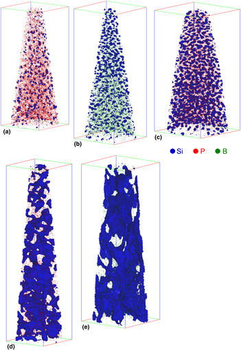
We analyze phosphorus (P)- and boron (B)-doped silicon nanocrystals (Si NCs) with various compositions of silicon-rich oxide using atom probe tomography. By creating Si iso-concentration surfaces, it is confirmed that there are two types of Si NC networks depending on the amount of excess Si. A proximity histogram shows that P prefers to locate inside the Si NCs, whereas B is more likely to reside outside the Si NCs. We discuss the difference in a preferential location between P and B by a segregation coefficient.

Type
Research Letters
Copyright
Copyright © Materials Research Society 2016 

Access options

Get access to the full version of this content by using one of the access options below. (Log in options will check for institutional or personal access. Content may require purchase if you do not have access.)

References

1. Conibeer, G., Green, M., Cho, E.-C., König, D., Cho, Y.-H., Fangsuwannarak, T., Scardera, G., Pink, E., Huang, Y., Puzzer, T., Huang, S., Song, D., Flynn, C., Park, S., Hao, X., and Mansfield, D.: Silicon quantum dot nanostructures for tandem photovoltaic cells. Thin Solid Films 516, 6748 (2008).Google Scholar
2. Sugimoto, H., Fujii, M., Imakita, K., Hayashi, S., and Akamatsu, K.: Phosphorus and boron codoped colloidal silicon nanocrystals with inorganic atomic ligands. J. Phys. Chem. C 117, 6807 (2013).CrossRefGoogle Scholar
3. Jiang, C.-W. and Green, M.A.: Silicon quantum dot superlattices: modeling of energy bands, densities of states, and mobilities for silicon tandem solar cell applications. J. Appl. Phys. 99, 114902 (2006).Google Scholar
4. Dalpian, G.M. and Chelikowsky, J.R.: Self-purification in semiconductor Nanocrystals. Phys. Rev. Lett. 96, 226802 (2006).Google Scholar
5. Fujii, M., Mimura, A., Hayashi, S., and Yamamoto, K.: Photoluminescence from Si nanocrystals dispersed in phosphosilicate glass thin films: improvement of photoluminescence efficiency. Appl. Phys. Lett. 75, 185 (1999).Google Scholar
6. Zacharias, M., Heitmann, J., Scholz, R., Kahler, U., Schmidt, M., and Bläsing, J.: Size-controlled highly luminescent silicon nanocrystals: a SiO/SiO2 superlattice approach. Appl. Phys. Lett. 80, 661 (2002).CrossRefGoogle Scholar
7. Conibeer, G., Green, M.A., König, D., Perez-Wurfl, I., Huang, S., Hao, X., Di, D., Shi, L., Shrestha, S., Puthen-Veetil, B., So, Y., Zhang, B., and Wan, Z.: Silicon quantum dot based solar cells: addressing the issues of doping, voltage and current transport. Prog. Photovolt: Res. Appl. 19, 813 (2011).Google Scholar
8. Gault, B., Moody, M.P., Cairney, J.M., and Ringer, S.P.: Atom Probe Microscopy (Springer, New York, 2012).Google Scholar
9. Fujii, M., Hayashi, S., and Yamamoto, K.: Photoluminescence from B-doped Si nanocrystals. J. Appl. Phys. 83, 7953 (1998).CrossRefGoogle Scholar
10. Hernández, S., López-Vidrier, J., López-Conesa, L., Hiller, D., Gutsch, S., Ibáñez, J., Estradé, S., Peiró, F., Zacharias, M., and Garrido, B.: Determining the crystalline degree of silicon nanoclusters/SiO2 multilayers by Raman scattering. J. Appl. Phys. 115, 203504 (2014).CrossRefGoogle Scholar
11. Yang, T.C.-J., Nomoto, K., Lin, Z., Wu, L., Puthen-Veettil, B., Zhang, T., Jia, X., Conibeer, G., and Perez-Wurfl, I.: High Si Content SRO/SiO2 Bilayer Superlattices with Boron and Phosphorus Doping for Next Generation Si Quantum Dot Photovoltaics. in Proceedings of the 42nd IEEE Photovoltaic Specialists Conference doi: 10.1109/PVSC.2015.7355967 (2015).Google Scholar
12. Felfer, P.J., Alam, T., Ringer, S.P., and Cairney, J.M.: A reproducible method for damage-free site-specific preparation of atom probe tips from interfaces. Mirosc. Res. Techn. 75, 484 (2012).Google Scholar
13. Vurpillot, F., Gault, B., Geiser, B.P., and Larson, D.J.: Reconstructing atom probe data: a review. Ultramicroscopy 132, 19 (2013).Google Scholar
14. Hellman, O.C., Vandenbroucke, J.A., Rusing, J., Isheim, D., and Seidman, D.N.: Analysis of three-dimensional atom-probe data by the Proximity Histogram. Microsc. Microanal. 6, 437 (2000).Google Scholar
15. Hartel, A.M., Hiller, D., Gutsch, S., Löper, P., Estradé, S., Peiró, F., Garrido, B., and Zacharias, M.. Formation of size-controlled silicon nanocrystals in plasma enhanced chemical vapor deposition grown SiOxNy/SiO2 superlattices. Thin Solid Films 520, 121 (2011).Google Scholar
16. Mulloni, V., Bellutti, P., and Vanzetti, L.: XPS and SIMS investigation on the role of nitrogen in Si nanocrystals formation. Surf. Sci. 585, 137 (2005).Google Scholar
17. Sarikov, A., Litovchenko, V., Lisovskyy, I., Maidanchuk, I., and Zlobin, S.: Role of oxygen migration in the kinetics of the phase separation of nonstoichiometric silicon oxide films during high-temperature annealing. Appl. Phys. Lett. 91, 133109 (2007).CrossRefGoogle Scholar
18. Hiller, D., Gutsch, S., Hartel, A.M., Löper, P., Gebel, T., and Zacharias, M.: A low thermal impact annealing process for SiO2-embedded Si nanocrystals with optimized interface quality. J. Appl. Phys. 115, 134311 (2014).Google Scholar
19. Laube, J., Gutsch, S., Wang, D., Zacharias, M., and Hiller, D.: Two-dimensional percolation threshold in confined Si nanoparticle networks. Appl. Phys. Lett. 108, 043106 (2016).Google Scholar
20. Trumbore, F.A.: Solid solubilities of impurity elements in Germanium and silicon. Bell Syst. Tech. J. 39, 205 (1960).CrossRefGoogle Scholar
21. Olesinski, R.W., Kanani, N., and Abbaschian, G.J.: The P-Si (Phosphorus-Silicon) system. Bull. Alloy Phase Diagr. 6, 130 (1985).Google Scholar
22. Olesinski, R.W. and Abbaschian, G.J.: The B-Si (Boron-Silicon) system. Bull. Alloy Phase Diagr. 5, 478 (1984).CrossRefGoogle Scholar
23. Sumida, K., Ninomiya, K., Fujii, M., Fujio, K., Hayashi, S., Kodama, M., and Ohta, H.: Electron spin-resonance studies of conduction electrons in phosphorus-doped silicon nanocrystals. J. Appl. Phys. 101, 033504 (2007).Google Scholar
24. Ghezzo, M. and Brown, D.M.: Diffusivity summary of B, Ga, P, As, and Sb in SiO2 . J. Electrochem. Soc. 120, 146 (1973).Google Scholar
25. Fair, R.B. and Tsai, J.C.C.: A quantitative model for the diffusion of phosphorus in silicon and the emitter dip effect. J. Electrochem. Soc. 124, 1107 (1977).Google Scholar
26. Fair, R.B.: Boron diffusion in silicon-concentration and orientation dependence, background effects, and profile estimation. J. Electrochem. Soc. 122, 800 (1975).Google Scholar
27. Hadjisavvas, G. and Kelires, P.C.: Structure and energetics of Si Nanocrystals embedded in a-SiO2. Phys. Rev. Lett. 93, 226104 (2004).Google Scholar
28. Sakamoto, K., Nishi, K., Ichikawa, F., and Ushio, S.: Segregation and transport coefficients of impurities at the Si/SiO2 interface. J. Appl. Phys. 61, 1553 (1987).CrossRefGoogle Scholar
29. Fukata, N., Ishida, S., Yokono, S., Takiguchi, R., Chen, J., Sekiguchi, T., and Murakami, K.: Segregation behaviors and radial distribution of Dopant atoms in silicon nanowires. Nano Lett. 11, 651 (2011).CrossRefGoogle ScholarPubMed
30. Grove, A.S., Leistiko, O., and Sah, C.T.J.: Redistribution of acceptor and donor impurities during thermal oxidation of silicon. J. Appl. Phys. 35, 2695 (1964).Google Scholar