Hostname: page-component-745bb68f8f-b6zl4 Total loading time: 0 Render date: 2025-01-12T15:42:52.723Z Has data issue: false hasContentIssue false

Rapid liftoff of epitaxial thin films

Published online by Cambridge University Press:  20 August 2013
Garrett J. Hayes*
Affiliation:
Department of Materials Science & Engineering, Stanford University, Stanford, California 94305
Bruce M. Clemens
Affiliation:
Department of Materials Science & Engineering, Stanford University, Stanford, California 94305
*
a)Address all correspondence to this author. e-mail: ghayes@stanford.edu
Get access

Abstract

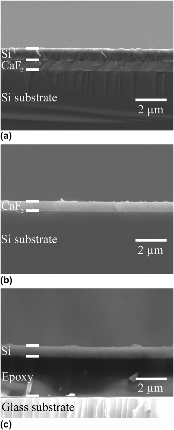
Electronic devices made from single crystal thin films attached to inexpensive support substrates offer reduced material costs compared to wafer-based devices; however, scalable and inexpensive processes for producing these single crystal film structures have remained elusive. In this work, we describe a new approach for fabricating these structures. In our approach, an epitaxial film is grown on a single crystal template and is then separated from its growth surface via fracture along a weak heteroepitaxial interface between the single crystal film and its growth substrate. We show that epitaxial films of Si, Ge, and GaAs, with thicknesses ranging from 100 nm to 1 μm, grown on epitaxial CaF2 overlayers on Si <111> substrates, can be transferred to glass substrates by inducing fracture along the heteroepitaxial interface between the semiconductor film and CaF2, or between CaF2 and the Si wafer, assisted by the presence of water as in moisture-assisted cracking.

Type
Articles
Copyright
Copyright © Materials Research Society 2013 

Access options

Get access to the full version of this content by using one of the access options below. (Log in options will check for institutional or personal access. Content may require purchase if you do not have access.)

References

REFERENCES

Brendel, R.: A novel process for ultrathin monocrystalline silicon solar cells on glass. 14th European Photovoltaic Solar Energy Conference Proceeding, Vol. 1354, Barcelona, Spain, June 30–July 4, 1997.Google Scholar
Rao, R.A., Mathew, L., Saha, S., Smith, S., Sarkar, D., Garcia, R., Stout, R., Gurmu, A., Onyegam, E., and Ahn, D.: A novel low cost 25μm thin exfoliated monocrystalline Si solar cell technology. 37th IEEE Photovoltaic Specialists Conference (PVSC), Seattle, WA, June 19–24, 2011; pp. 001504001507.CrossRefGoogle Scholar
Bedell, S.W., Shahrjerdi, D., Hekmatshoar, B., Fogel, K., Lauro, P.A., Ott, J.A., Sosa, N., and Sadana, D.: Kerf-less removal of Si, Ge, and III-V layers by controlled spalling to enable low-cost PV technologies. IEEE J. Photovoltaics 2, 141147 (2012).CrossRefGoogle Scholar
Martini, R., Gonzalez, M., Dross, F., Masolin, A., Vaes, J., Frederickx, D., and Poortmans, J.: Epoxy-induced spalling of silicon. Energy Procedia 27, 567572 (2012).CrossRefGoogle Scholar
Bruel, M.: Silicon on insulator material technology. Electron. Lett. 31, 12011202 (1995).CrossRefGoogle Scholar
Yablonovitch, E., Gmitter, T., Harbison, J.P., and Bhat, R.: Extreme selectivity in the lift-off of epitaxial GaAs films. Appl. Phys. Lett. 51, 2222 (1987).CrossRefGoogle Scholar
Schermer, J.J., Mulder, P., Bauhuis, G.J., Voncken, M.M.A.J., van Deelen, J., Haverkamp, E., and Larsen, P.K.: Epitaxial lift-off for large area thin film III/V devices. Phys. Status Solidi A 202, 501508 (2005).CrossRefGoogle Scholar
Anderson, T.L.: Fracture Mechanics: Fundamentals and Applications, 3rd ed. (CRC Press, Boca Raton, FL, 2005), pp. 25100.CrossRefGoogle Scholar
Schumann, B. and Neumann, H.: Thermal expansion of CaF2 from 298 to 1173 K. Cryst. Res. Technol. 19, K13K14 (1984).CrossRefGoogle Scholar
Slack, G.A. and Bartram, S.F.: Thermal expansion of some diamondlike crystals. J. Appl. Phys. 46, 8998 (1975).CrossRefGoogle Scholar
Olmstead, M.A. and Bringans, R.D.: Initial stages of epitaxial semiconductor-insulator heterointerface formation. J. Electron. Spectrosc. Relat. Phenom. 51, 599612 (1990).CrossRefGoogle Scholar
Schroeder, B.R., Meng, S., Bostwick, A., Olmstead, M.A., and Rotenberg, E.: Epitaxial growth of laminar crystalline silicon on CaF2. Appl. Phys. Lett. 77, 12891291 (2000).CrossRefGoogle Scholar
Wang, C.R., Bierkandt, M., Paprotta, S., Wietler, T., and Hofmann, K.R.: CaF2/Si/CaF2 resonant tunneling diodes grown by B surfactant-mediated epitaxy. Appl. Phys. Lett. 86, 033111 (2005).CrossRefGoogle Scholar
Kawasaki, K. and Tsutsui, K.: Heteroepitaxy of GaAs on CaF2/Si (111) by surface free energy modulation method. Mater. Res. Soc. Symp. Proc. 535, 5158 (1999).CrossRefGoogle Scholar
Sinharoy, S.: Fluoride/semiconductor and semiconductor/fluoride/semiconductor heteroepitaxial structure research: A review. Thin Solid Films 187, 231243 (1990).CrossRefGoogle Scholar